End of the Road: An AnandTech Farewell
It is with great sadness that I find myself penning the hardest news post I’ve ever needed to write here at AnandTech. After over 27 years of covering the wide – and wild – world of computing hardware, today is AnandTech’s final day of publication.
For better or worse, we’ve reached the end of a long journey – one that started with a review of an AMD processor, and has ended with the review of an AMD processor. It’s fittingly poetic, but it is also a testament to the fact that we’ve spent the last 27 years doing what we love, covering the chips that are the lifeblood of the computing industry.
A lot of things have changed in the last quarter-century – in 1997 NVIDIA had yet to even coin the term “GPU” – and we’ve been fortunate to watch the world of hardware continue to evolve over the time period. We’ve gone from boxy desktop computers and laptops that today we’d charitably classify as portable desktops, to pocket computers where even the cheapest budget device puts the fastest PC of 1997 to shame.
The years have also brought some monumental changes to the world of publishing. AnandTech was hardly the first hardware enthusiast website, nor will we be the last. But we were fortunate to thrive in the past couple of decades, when so many of our peers did not, thanks to a combination of hard work, strategic investments in people and products, even more hard work, and the support of our many friends, colleagues, and readers.
Still, few things last forever, and the market for written tech journalism is not what it once was – nor will it ever be again. So, the time has come for AnandTech to wrap up its work, and let the next generation of tech journalists take their place within the zeitgeist.
It has been my immense privilege to write for AnandTech for the past 19 years – and to manage it as its editor-in-chief for the past decade. And while I carry more than a bit of remorse in being AnandTech’s final boss, I can at least take pride in everything we’ve accomplished over the years, whether it’s lauding some legendary products, writing technology primers that still remain relevant today, or watching new stars rise in expected places. There is still more that I had wanted AnandTech to do, but after 21,500 articles, this was a good start.
And while the AnandTech staff is riding off into the sunset, I am happy to report that the site itself won’t be going anywhere for a while. Our publisher, Future PLC, will be keeping the AnandTech website and its many articles live indefinitely. So that all of the content we’ve created over the years remains accessible and citable. Even without new articles to add to the collection, I expect that many of the things we’ve written over the past couple of decades will remain relevant for years to come – and remain accessible just as long.
The AnandTech Forums will also continue to be operated by Future’s community team and our dedicated troop of moderators. With forum threads going back to 1999 (and some active members just as long), the forums have a history almost as long and as storied as AnandTech itself (wounded monitor children, anyone?). So even when AnandTech is no longer publishing articles, we’ll still have a place for everyone to talk about the latest in technology – and have those discussions last longer than 48 hours.
Finally, for everyone who still needs their technical writing fix, our formidable opposition of the last 27 years and fellow Future brand, Tom’s Hardware, is continuing to cover the world of technology. There are a couple of familiar AnandTech faces already over there providing their accumulated expertise, and the site will continue doing its best to provide a written take on technology news.
So Many Thank Yous
As I look back on everything AnandTech has accomplished over the past 27 years, there are more than a few people, groups, and companies that I would like to thank on behalf of both myself and AnandTech as a whole.
First and foremost, I cannot thank enough all the editors who have worked for AnandTech over the years. There are far more of you than I can ever name, but AnandTech’s editors have been the lifeblood of the site, bringing over their expertise and passion to craft the kind of deep, investigative articles that AnandTech is best known for. These are the finest people I’ve ever had the opportunity to work with, and it shouldn’t come as any surprise that these people have become even bigger successes in their respective fields. Whether it’s hardware and software development, consulting and business analysis, or even launching rockets into space, they’ve all been rock stars whom I’ve been fortunate to work with over the past couple of decades.
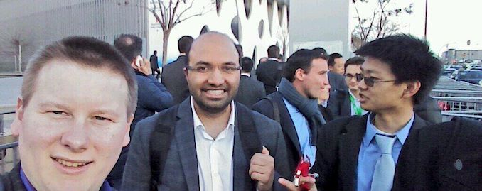
Ian Cutress, Anton Shilov, and Gavin Bonshor at Computex 2019
And a special shout out to the final class of AnandTech editors, who have been with us until the end, providing the final articles that grace this site. Gavin Bonshor, Ganesh TS, E. Fylladitakis, and Anton Shilov have all gone above and beyond to meet impossible deadlines and go half-way around the world to report on the latest in technology.
Of course, none of this would have been possible without the man himself, Anand Lal Shimpi, who started this site out of his bedroom 27 years ago. While Anand retired from the world of tech journalism a decade ago, the standard he set for quality and the lessons he taught all of us have continued to resonate within AnandTech to this very day. And while it would be tautological to say that there would be no AnandTech without Anand, it’s none the less true – the mark on the tech publishing industry that we’ve been able to make all started with him.
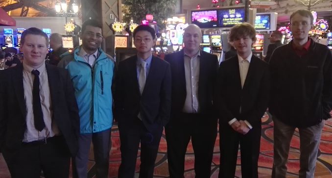
MWC 2014: Ian Cutress, Anand Lal Shimpi, Joshua Ho
I also want to thank the many, many hardware and software companies we’ve worked with over the years. More than just providing us review samples and technical support, we’ve been given unique access to some of the greatest engineers in the industry. People who have built some of the most complex chips ever made, and casually forgotten more about the subject than we as tech journalists will ever know. So being able to ask those minds stupid questions, and seeing the gears turn in their heads as they explain their ideas, innovations, and thought processes has been nothing short of an incredible learning experience. We haven’t always (or even often) seen eye-to-eye on matters with all of the companies we've covered, but as the last 27 years have shown, sharing the amazing advancements behind the latest technologies has benefited everyone, consumers and companies alike.
Thank yous are also due to AnandTech’s publishers over the years – Future PLC, and Purch before them. AnandTech’s publishers have given us an incredible degree of latitude to do things the AnandTech way, even when it meant taking big risks or not following the latest trend. A more cynical and controlling publisher could have undoubtedly found ways to make more money from the AnandTech website, but the resulting content would not have been AnandTech. We’ve enjoyed complete editorial freedom up to our final day, and that’s not something so many other websites have had the luxury to experience. And for that I am thankful.
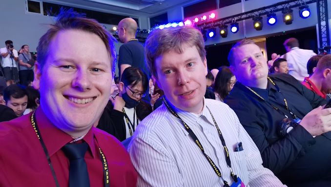
CES 2016: Ian Cutress, Ganesh TS, Joshua Ho, Brett Howse, Brandon Chester, Billy Tallis
Finally, I cannot thank our many readers enough. Whether you’ve been following AnandTech since 1997 or you’ve just recently discovered us, everything we’ve published here we’ve done for you. To show you what amazing things were going on in the world of technology, the radical innovations driving the next generation of products, or a sober review that reminds us all that there’s (almost) no such thing as bad products, just bad pricing. Our readers have kept us on our toes, pushing us to do better, and holding us responsible when we’ve strayed from our responsibilities.
Ultimately, a website is only as influential as its readers, otherwise we would be screaming into the void that is the Internet. For all the credit we can claim as writers, all of that pales in comparison to our readers who have enjoyed our content, referenced it, and shared it with the world. So from the bottom of my heart, thank you for sticking with us for the past 27 years.
Continuing the Fight Against the Cable TV-ification of the Web
Finally, I’d like to end this piece with a comment on the Cable TV-ification of the web. A core belief that Anand and I have held dear for years, and is still on our About page to this day, is AnandTech’s rebuke of sensationalism, link baiting, and the path to shallow 10-o'clock-news reporting. It has been our mission over the past 27 years to inform and educate our readers by providing high-quality content – and while we’re no longer going to be able to fulfill that role, the need for quality, in-depth reporting has not changed. If anything, the need has increased as social media and changing advertising landscapes have made shallow, sensationalistic reporting all the more lucrative.
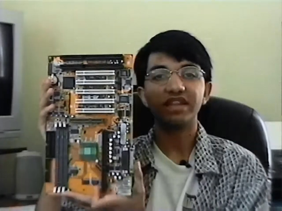
Speaking of TV: Anand Hosting The AGN Hardware Show (June 1998)
For all the tech journalists out there right now – or tech journalists to be – I implore you to remain true to yourself, and to your readers' needs. In-depth reporting isn’t always as sexy or as exciting as other avenues, but now, more than ever, it’s necessary to counter sensationalism and cynicism with high-quality reporting and testing that is used to support thoughtful conclusions. To quote Anand: “I don't believe the web needs to be academic reporting or sensationalist garbage - as long as there's a balance, I'm happy.”
Signing Off One Last Time
Wrapping things up, it has been my privilege over the last 19 years to write for one of the most impactful tech news websites that has ever existed. And while I’m heartbroken that we’re at the end of AnandTech’s 27-year journey, I can take solace in everything we’ve been able to accomplish over the years. All of which has been made possible thanks to our industry partners and our awesome readers.
On a personal note, this has been my dream job; to say I’ve been fortunate would be an understatement. And while I’ll no longer be the editor-in-chief of AnandTech, I’m far from being done with technology as a whole. I’ll still be around on Twitter/X, and we’ll see where my own journey takes me next.


To everyone who has followed AnandTech over the years, fans, foes, readers, competitors, academics, engineers, and just the technologically curious who want to learn a bit more about their favorite hardware, thank you for all of your patronage over the years. We could not have accomplished this without your support.
-Thanks,
Ryan Smith