Vue lecture

Il y a de nouveaux articles disponibles, cliquez pour rafraîchir la page.

Crucial T705 Gen5 NVMe SSD: A 14.5 GBps Consumer Flagship with 2400 MT/s 232L NAND

Crucial is unveiling the latest addition to its Gen5 consumer NVMe SSD lineup today - the T705 PCIe 5.0 M.2 2280 NVMe SSD. It takes over flagship duties from the Crucial T700 released last year. The company has been putting focus on the high-end consumer SSD segment in the last few quarters. The T700 was one of the first to offer more than 12 GBps read speeds, and the T705 being launched today is one of the first drives available for purchase in the 14+ GBps read speeds category.

The Crucial T705 utilizes the same platform as the T700 from last year - Phison's E26 controller with Micron's B58R 232L 3D TLC NAND. The key difference is the B58R NAND operating at 2400 MT/s in the new T705 (compared to the 2000 MT/s in the T700). Micron's 232L NAND process has now matured enough for the company to put out 2400 MT/s versions with enough margins. Similar to the T700, this drive is targeted towards gamers, content creators, and professional users as well as data-heavy AI use-cases.

The move to 2400 MT/s NAND has allowed Crucial to claim an increase in the performance of the drive in all four corners - up to 20% faster random writes, and 18% higher sequential reads. Additionally, Crucial also claims more bandwidth in a similar power window for the new drive.

The T705 is launching in three capacities - 1TB, 2TB, and 4TB. Both heatsink and non-heatsink versions are available. Crucial is also offering a white heatsink limited edition for the 2TB version. This caters to users with white-themed motherboards that are increasingly gaining market presence.

Phison has been pushing DirectStorage optimizations in its high-end controllers, and it is no surprise that the T705 advertises the use of Phison's 'I/O+ Technology' to appeal to gamers. Given its high-performance nature, it is no surprise that the E26 controller needs to be equipped with DRAM for managing the flash translation layer (FTL). Crucial is using Micron LPDDR4 DRAM (1GB / TB of flash) in the T705 for this purpose.

Crucial T705 Gen5 NVMe SSD Specifications
Capacity 1 TB 2 TB 4 TB
Model Numbers CT1000T705SSD3 (Non-Heatsink)
CT1000T705SSD5 (Heatsink)
CT2000T705SSD3 (Non-Heatsink)
CT2000T705SSD5 (Black Heatsink)
CT2000T705SSD5A (White Heatsink)
CT4000T705SSD3 (Non-Heatsink)
CT4000T705SSD5 (Heatsink)
Controller Phison PS5026-E26
NAND Flash Micron B58R 232L 3D TLC NAND at 2400 MT/s
Form-Factor, Interface Double-Sided M.2-2280, PCIe 5.0 x4, NVMe 2.0
Sequential Read 13600 MB/s 14500 MB/s 14100 MB/s
Sequential Write 10200 MB/s 12700 MB/s 12600 MB/s
Random Read IOPS 1.4 M 1.55 M 1.5 M
Random Write IOPS 1.75 M 1.8 M 1.8 M
SLC Caching Dynamic (up to 11% of user capacity)
TCG Opal Encryption Yes
Warranty 5 years
Write Endurance 600 TBW
0.33 DWPD
1200 TBW
0.33 DWPD
2400 TBW
0.33 DWPD
MSRP $240 (24¢/GB) (Non- Heatsink)
$260 (26¢/GB) (Heatsink)
$400 (20¢/GB) (Non- Heatsink)
$440 (22¢/GB) (Black Heatsink)
$484 (24.2¢/GB) (White Heatsink)
$714 (17.85¢/GB) (Non- Heatsink)
$730 (18.25¢/GB) (Heatsink)

Crucial is confident that the supplied passive heatsink is enough to keep the T705 from heavy throttling under extended use. The firmware throttling kicks in at 81C and protective shutdown at 90C. Flash pricing is not quite as low as it was last year, and the 2400 MT/s flash allows Micron / Crucial to place a premium on the product. At the 4TB capacity point, the drive can be purchased for as low as 18¢/GB, but the traditional 1TB and 2TB ones go for 20 - 26 ¢/GB depending on the heatsink option.

There are a number of Gen5 consumer SSDs slated to appear in the market over the next few months using the same 2400 MT/s B58R 3D TLC NAND and Phison's E26 controller (Sabrent's Rocket 5 is one such drive). The Crucial / Micron vertical integration on the NAND front may offer some advantage for the T705 when it comes to the pricing aspect against such SSDs. That said, the Gen5 consumer SSD market is still in its infancy with only one mass market (Phison E26) controller in the picture. The rise in consumer demand for these high-performance SSDs may coincide with other vendors such as Innogrit (with their IG5666) and Silicon Motion (with their SM2508) gaining traction. Currently, Crucial / Micron (with their Phison partnership) is the only Tier-1 vendor with a high-performance consumer Gen5 SSD portfolio, and the T705 cements their leadership position in the category further.

The Intel IFS Direct Connect 2024 Keynote (Starts at 8:30am PT/16:30 UTC)

This morning, Intel is set to provide updates on its foundry business (IFS) and process roadmap at its IFS Direct Connect event in Santa Clara. Intel is expected to unveil plans for how the company will transform the foundry industry and how it is set to become the world's first and only fully integrated systems foundry in the AI space. Led by Intel CEO Pat Gelsinger and Stuart Pann, the Senior Vice President and General Manager of Intel Foundry Services, both will deliver the event's opening keynote. Expected guests throughout the keynote include Sam Altman, the co-founder and CEO of OpenAI, Gina Raimondo, the US Secretary of Commerce, and Satya Nadella, the Chairman and CEO of Microsoft.

Join us at 8:30 am PT/16:30 pm UTC.

Arm Announces Neoverse V3 and N3 CPU Cores: Building Bigger and Moving Faster with CSS

A bit over 5 years ago, Arm announced their Neoverse initiative for server, cloud, and infrastructure CPU cores. Doubling-down on their efforts to break into the infrastructure CPU market in a big way, the company set about an ambitious multi-year plan to develop what would become a trio of CPU core lineups to address different segments of the market – ranging  from the powerful V series to the petite E series core. And while things have gone a little differently than Arm initially projected, they’re hardly in a position to complain, as the Neoverse line of CPU cores has never been as successful as it is now. Custom CPU designs based on Neoverse cores are all the rage with cloud providers, and the broader infrastructure market has seen its own surge.

Now, as the company and its customers turn towards 2024 and a compute market that is in the throes of another transformative change due to insatiable demand for AI hardware, Arm is preparing to release its next generation of Neoverse CPU core designs to its customers. And in the process, the company is reaching the culmination of the original Neoverse roadmap.

This morning the company is taking the wraps off of the V3 CPU architecture (codename Poseidon) for high-performance systems, as well as the N3 CPU architecture (codename Hermes) for balanced systems. These designs are now ready for customers to begin integrating into their own chip designs, with both the individual CPU core designs as well as the larger Neoverse Compute Subsystems (CSS) available. Between the various combinations of IP configurations, Arm is looking to offer something for everyone, and especially chip designers who are looking to integrate ready-made IP for a quick turnaround in developing their own chips.

With that said, it should be noted that today’s announcement is also a lighter one than what we’ve come to expect from previous Neoverse announcements. Arm isn’t releasing any of the deep architectural details on the new Neoverse platforms today, so while we have the high-level details on the hardware and some basic performance estimates, the underlying details on the CPU cores and their related plumbing is something Arm is keeping to themselves until a later time.

IFS Reborn as Intel Foundry: Expanded Foundry Business Adds 14A Process To Roadmap

5 nodes in 4 years. This is what Intel CEO Pat Gelsinger promised Intel’s customers, investors, and the world at large back in 2021, when he laid out Intel’s ambitious plan to regain leadership in the foundry space. After losing Intel’s long-held spot as the top fab in the world thanks to compounding delays in the 2010s, the then-new Intel CEO bucked calls from investors to sell off Intel’s fabs, and instead go all-in on fabs like Intel has never done before, to become a top-to-bottom foundry service for the entire world to use.

Now a bit over two years later, and Intel is just starting to see the first fruits from that aggressive roadmap, both in terms of technologies and customers. Products based on Intel’s first EUV-based node, Intel 4, are available in the market today, and its high-volume counterpart, Intel 3, is ready as well. Meanwhile, Intel is putting the final touches on its first Gate-All-Around (GAAFET)/RibbonFET for 2024 and 2025. It’s a heady time for the company, but it’s also a critical one. Intel has reached the point where they need to deliver on those promises – and they need to do so in a very visible way.

To that end, today Intel’s Foundry group – the artist formally known as Intel Foundry Services – is holding its first conference, Direct Connect. And even more than being a showcase for customers and press, this is Intel’s coming-out party for the fab industry as a whole, where Intel’s foundry (and only Intel’s foundry) gets the spotlight, a rarity in the massive business that is Intel.

Arm and Samsung to Co-Develop 2nm GAA-Optimized Cortex Cores

Arm and Samsung this week announced their joint design-technology co-optimization (DTCO) program for Arm's next-generation Cortex general-purpose CPU cores as well as Samsung's next-generation process technology featuring gate-all-around (GAA) multi-bridge-channel field-effect transistors (MBCFETs). 

"Optimizing Cortex-X and Cortex-A processors on the latest Samsung process node underscores our shared vision to redefine what’s possible in mobile computing, and we look forward to continuing to push boundaries to meet the relentless performance and efficiency demands of the AI era," said Chris Bergey, SVP and GM, Client Business at Arm.

Under the program, the companies aim to deliver tailored versions of Cortex-A and Cortex-X cores made on Samsung's 2 nm-class process technology for various applications, including smartphones, datacenters, infrastructure, and various customized system-on-chips. For now, the companies does not say whether they aim to co-optimize Arm's Cortex cores for Samsung's 1st generation 2 nm production node called SF2 (due in 2025), or the plan is to optimize these cores for all SF2-series technologies, including SF2 and SF2P.

GAA nanosheet transistors with channels that are surrounded by gates on all four sides have a lot of options for optimization. For example, nanosheet channels can be widened to increase drive current and boost performance or shrunken to reduce power consumption and cost. Depending on the application, Arm and Samsung will have plenty of design choices.

Keeping in mind that we are talking about Cortex-A cores aimed at a wide variety of applications as well as Cortex-X cores designed specifically to deliver maximum performance, the results of the collaborative work promise to be quite decent. In particular, we are looking forward Cortex-X cores with maximized performance, Cortex-A cores with optimized performance and power consumption, and Cortex-A cores with reduced power consumption.

Nowadays collaboration between IP (intellectual property) developers, such as Arm, and foundries, such as Samsung Foundry, is essential to maximize performance, reduce power consumption, and optimize transistor density. The joint work with Arm will ensure that Samsung's foundry partners will have access to processor cores that can deliver exactly what they need.

AMD CEO Dr. Lisa Su to Deliver Opening Keynote at Computex 2024

Taiwan External Trade Development Council (TAITRA), the organizer of Computex, announced today that Dr. Lisa Su, AMD's chief executive officer, will give the trade show's Opening Keynote. Su's speech is set for the morning of June 3, 2024, shortly before the formal start of the show. According to AMD, the keynote talk will be "highlighting the next generation of AMD products enabling new experiences and breakthrough AI capabilities from the cloud to the edge, PCs and intelligent end devices."

This year's Computex is focused on six key areas: AI computing, Advanced Connectivity, Future Mobility, Immersive Reality, Sustainability, and Innovations. Being a leading developer of CPUs, AI and HPC GPUs, consumer GPUs, and DPUs, AMD can talk most of these topics quite applicably.

As AMD is already mid-cycle on most of their product architectures, the company's most recent public roadmaps have them set to deliver major new CPU and GPU architectures before the end of 2024 with Zen 5 CPUs and RDNA 4 GPUs, respectively. AMD has not previously given any finer guidance on when in the year to expect this hardware, though AMD's overall plans for 2024 are notably more aggressive than the start of their last architecture cycle in 2022. Of note, the company has previously indicated that it intends to launch all 3 flavors of the Zen 5 architecture this year – not just the basic core, but also Zen 5c and Zen 5 with V-Cache – as well as a new mobile SoC (Strix Point). By comparison, it took AMD well into 2023 to do the same with Zen 4 after starting with a fall 2022 launch for those first products.


AMD 2022 Financial Analyst Day CPU Core Roadmap

This upcoming keynote will be Lisa Su's third Computex keynote after her speeches at Computex 2019 and Computex 2022. In both cases she also announced upcoming AMD products.

In 2019, she showcased performance improvements of then upcoming 3rd Generation Ryzen desktop processors and 7nm EPYC datacenter processors. Lisa Su also highlighted AMD's advancements in 7nm process technology, showcasing the world's first 7nm gaming GPU, the Radeon VII, and the first 7nm datacenter GPU, the Radeon Instinct MI60.

In 2022, the head of AMD offered a sneak peek at the then-upcoming Ryzen 7000-series desktop processors based on the Zen 4 architecture, promising significant performance improvements. She also teased the next generation of Radeon RX 7000-series GPUs with the RDNA 3 architecture.

AMD Fixed the STAPM Throttling Issue, So We Retested The Ryzen 7 8700G and Ryzen 5 8600G

When we initially reviewed the latest Ryzen 8000G APUs from AMD last month, the Ryzen 7 8700G and Ryzen 5 8600G, we became aware of an issue that caused the APUs to throttle after a few minutes. This posed an issue for a couple of reasons, the first being it compromised our data to reflect the true capabilities of the processors, and the second, it highlighted an issue that AMD forgot to disable from their mobile series of Pheonix chips (Ryzen 7040) when implementing it over to the desktop.

We updated the data in our review of the Ryzen 7 8700G and Ryzen 5 8600G to reflect performance with STAPM on the initial firmware and with STAPM removed with the latest firmware. Our updated and full review can be accessed by clicking the link below:

As we highlighted in our Ryzen 8000G APU STAPM Throttling article, AMD, through AM5 motherboard vendors such as ASUS, has implemented updated firmware that removes the STAPM limitation. Just to quickly recap the Skin Temperature-Aware Power Management (STAPM) feature and what it does, AMD introduced it in 2014. STAPM itself is a feature implemented into their mobile processors. It is designed to extend the on-die power management by considering the processor's internal temperatures taken by on-chip thermal diodes and the laptop's surface temperature (i.e., the skin temperature).

The aim of STAPM is to prevent laptops from becoming uncomfortably warm for users, allowing the processor to actively throttle back its heat generation based on the thermal parameters between the chassis and the processor itself. The fundamental issue with STAPM in the case of the Ryzen 8000G APUs, including the Ryzen 7 8700G and Ryzen 5 8600G, is that these are mobile processors packaged into a format for use with the AM5 desktop platform. As a desktop platform is built into a chassis that isn't placed on a user's lap, the STAPM feature becomes irrelevant.

As we saw when we ran a gaming load over a prolonged period of time on the Ryzen 7 8700G with the firmware available at launch, we hit power throttling (STAPM) after around 3 minutes. As we can see in the above chart, power dropped from a sustained value of 83-84 W down to around 65 W, representing a drop in power of around 22%. While we know Zen 4 is a very efficient architecture at lower power values, overall performance will drop once this limit is hit. Unfortunately, AMD forgot to remove STAPM limits when transitioning Pheonix to the AM5 platform.

Retesting the same game (F1 2023) at the same settings (720p High) with the firmware highlighting that STAPM had been removed, we can see that we aren't experiencing any of the power throttling we initially saw. We can see power is sustained for over 10 minutes of testing (we did test for double this), and we saw no drops in package power, at least not from anything related to STAPM. This means for users on the latest firmware on whatever AM5 motherboard is being used, power and, ultimately, performance remain consistent with what the Ryzen 7 8700G should have been getting at launch.

The key question is, does removing the STAPM impact our initial results in our review of the Ryzen 7 8700G and Ryzen 5 8600G? And if so, by how much, or if at all? We added the new data to our review of the Ryzen 7 8700G and Ryzen 5 8600G but kept the initial results so that users can see if there are any differences in performance. Ultimately, benchmark runs are limited to the time it takes to run them, but in real-world scenarios, tasks such as video rendering and longer sustained loads are more likely to show gains in performance. After all, a drop of 22% in power is considerable, especially over a task that could take an hour.

(4-1d) Blender 3.6: Pabellon Barcelona (CPU Only)

Using one of our longer benchmarks, such as Blender 3.6, to highlight where performance gains are notable when using the latest firmware with the STAPM limitations removed, we saw an increase in performance of around 7.5% on the Ryzen 7 8700G with this removed. In the same benchmark, we saw an increase of around 4% on the Ryzen 5 8600G APU.

Over all of the Blender 3.6 tests in the rendering section of our CPU performance suite, performance gains hovered between 2 and 4.4% on the Ryzen 5 8600G, and between 5 and 7.5% on the Ryzen 8700G, which isn't really free performance, it's the performance that should have been there to begin with at launch.

IGP World of Tanks - 768p Min - Average FPS

Looking at how STAPM affected our initial data, we can see that the difference in World of Tanks at 768p Minumum settings had a marginal effect at best through STAPM by around 1%. Given how CPU-intensive World of Tanks is, and combining this with integrated graphics, the AMD Ryzen APUs (5000G and 8000G) both shine compared to Intel's integrated UHD graphics in gaming. Given that gaming benchmarks are typically time-limited runs, it's harder to identify performance gains. The key to takeaway here is that with the STAPM limitation removed, the performance shouldn't drop over sustained periods of time, so our figures above and our updated review data aren't compromised.

(i-3) Total War Warhammer 3 - 1440p Ultra - Average FPS

Regarding gaming with a discrete graphics card, we saw no drastic changes in performance, as highlighted by our Total War Warhammer 3 at 1440p Ultra benchmark. Across the board, in our discrete graphics results with both the Ryzen 7 8700G and the Ryzen 5 8600G, we saw nothing but marginal differences in performance (less than 1%). As we've mentioned, removing the STAPM limitations doesn't necessarily improve performance. Still, it allows the APUs to keep the same performance level for sustained periods, which is how it should have been at launch. With STAPM applied as with the initial firmware at launch on AM5 motherboards, power would drop by around 22%, limiting the full performance capability over prolonged periods.

As we've mentioned, we have updated our full review of the AMD Ryzen 7 8700G and Ryzen 5 8600G APUs to reflect our latest data gathered from testing on the latest firmware. Still, we can fully confirm that the STAPM issue has been fixed and that the performance is as it should be on both chips.

You can access all of our updated data in our review of the Ryzen 7 8700G and Ryzen 5 8600G by clicking the link below.

Intel Previews Sierra Forest with 288 E-Cores, Announces Granite Rapids-D for 2025 Launch at MWC 2024

At MWC 2024, Intel confirmed that Granite Rapids-D, the successor to Ice Lake-D processors, will come to market sometime in 2025. Furthermore, Intel also provided an update on the 6th Gen Xeon Family, codenamed Sierra Forest, which is set to launch later this year and will feature up to 288 cores designed for vRAN network operators to improve performance in boost per rack for 5G workloads.

These chips are designed for handling infrastructure, applications, and AI workloads and aim to capitalize on current and future AI and automation opportunities, enhancing operational efficiency and ownership costs in next-gen applications and reflecting Intel's vision of integrating 'AI Everywhere' across various infrastructures.

Intel Sierra Forest: Up to 288 Efficiency Cores, Set for 2H 2024

The first of Intel's announcements at MWC 2024 focuses on their upcoming Sierra Forest platform, which is scheduled for the 1st half of 2024. Initially announced in February 2022 during Intel's Investor Meeting, Intel is splitting its server roadmap into solutions featuring only performance (P) and efficiency (E) cores. We already know that Sierra Forest's new chips feature a full E-core architecture designed for maximum efficiency in scale-out, cloud-native, and contained environments.

These chips utilize CPU chiplets built on the Intel 3 process alongside twin I/O chiplets based on the Intel 7 node. This combination allows for a scalable architecture, which can accommodate increasing core counts by adding more chiplets, optimizing performance for complex computing environments.

Intel's Sierra Forest, Intel's full E-core designed Xeon processor family, is anticipated to significantly enhance power efficiency with up to 288 E-cores per socket. Intel also claims that Sierra Forest is expected to deliver 2.7 times the performance-per-rack compared to an unspecified platform from 2021; this could be either Ice Lake or Cascade Lake, but Intel didn't mention which.

Additionally, Intel is promising savings of up to 30% in Infrastructure Power Management with Sierra Forest as their Infrastructure Power Manager (IPM) application is now available commercially for 5G cores. Power manageability and efficiency are growing challenges for network operators, so IPM is designed to allow network operators to optimize energy efficiency and TCO savings.

Intel also includes vRAN, which is vital for modern mobile networks, and many operators are forgoing opting for specific hardware and instead leaning towards virtualized radio access networks (vRANs). Using vRAN Boost, which is an integrated accelerator within Xeon Processors, Intel states that the 4th Gen Xeon should be able to reduce power consumption by around 20% while doubling the available network capacity.

Intel's push for 'AI Everywhere' is also a constant focus here, with AI's role in vRAN management becoming more crucial. Intel has announced the vRAN AI Developer Kit, which is available to select partners. This allows partners and 5G network providers to develop AI models to optimize for vRAN applications, tailor their vRAN-based functions to more use cases, and adapt to changes within those scenarios.

Intel Granite Rapids-D: Coming in 2025 For Edge Solutions

Intel's Granite Rapids-D, designed for Edge solutions, is set to bolster Intel's role in virtual radio access network (vRAN) workloads in 2025. Intel also promises marked efficiency enhancements and some vRAN Boost optimizations similar to those expected on Sierra Forest. Set to follow on from the current Ice Lake-D for the edge; Intel is expected to use the performance (P) cores used within Granite Rapids server parts and optimize the V/F curve designed for the lower-powered Edge platform. As outlined by Intel, the previous 4th generation Xeon platform effectively doubled vRAN capacity, enhancing network capabilities while reducing power consumption by up to 20%.

Granite Rapids-D aims to further these advancements, utilizing Intel AVX for vRAN and integrated Intel vRAN Boost acceleration, thereby offering substantial cost and performance benefits on a global scale. While Intel hasn't provided a specific date (or month) of when we can expect to see Granite Rapids-D in 2025, Intel is currently in the process of sampling these next-gen Xeon-D processors with partners, aiming to ensure a market-ready platform at launch.

Related Reading

Micron Kicks Off Production of HBM3E Memory

Micron Technology on Monday said that it had initiated volume production of its HBM3E memory. The company's HBM3E known good stack dies (KGSDs) will be used for Nvidia's H200 compute GPU for artificial intelligence (AI) and high-performance computing (HPC) applications, which will ship in the second quarter of 2024.

Micron has announced it is mass-producing 24 GB 8-Hi HBM3E devices with a data transfer rate of 9.2 GT/s and a peak memory bandwidth of over 1.2 TB/s per device. Compared to HBM3, HBM3E increases data transfer rate and peak memory bandwidth by a whopping 44%, which is particularly important for bandwidth-hungry processors like Nvidia's H200.

Nvidia's H200 product relies on the Hopper architecture and offers the same computing performance as the H100. Meanwhile, it is equipped with 141 GB of HBM3E memory featuring bandwidth of up to 4.8 TB/s, a significant upgrade from 80 GB of HBM3 and up to 3.35 TB/s bandwidth in the case of the H100.

Micron's memory roadmap for AI is further solidified with the upcoming release of a 36 GB 12-Hi HBM3E product in March 2024. Meanwhile, it remains to be seen where those devices will be used.

Micron uses its 1β (1-beta) process technology to produce its HBM3E, which is a significant achievement for the company as it uses its latest production node for its data center-grade products, which is a testament to the manufacturing technology.

Starting mass production of HBM3E memory ahead of competitors SK Hynix and Samsung is a significant achievement for Micron, which currently holds a 10% market share in the HBM sector. This move is crucial for the company, as it allows Micron to introduce a premium product earlier than its rivals, potentially increasing its revenue and profit margins while gaining a larger market share.

"Micron is delivering a trifecta with this HBM3E milestone: time-to-market leadership, best-in-class industry performance, and a differentiated power efficiency profile," said Sumit Sadana, executive vice president and chief business officer at Micron Technology. "AI workloads are heavily reliant on memory bandwidth and capacity, and Micron is very well-positioned to support the significant AI growth ahead through our industry-leading HBM3E and HBM4 roadmap, as well as our full portfolio of DRAM and NAND solutions for AI applications."

Source: Micron

Samsung Launches 12-Hi 36GB HBM3E Memory Stacks with 10 GT/s Speed

Samsung announced late on Monday the completion of the development of its 12-Hi 36 GB HBM3E memory stacks, just hours after Micron said it had kicked off mass production of its 8-Hi 24 GB HBM3E memory products. The new memory packages, codenamed Shinebolt, increase peak bandwidth and capacity compared to their predecessors, codenamed Icebolt, by over 50% and are currently the world's fastest memory devices.

As the description suggests, Samsung's Shinebolt 12-Hi 36 GB HBM3E stacks pack 12 24Gb memory devices on top of a logic die featuring a 1024-bit interface. The new 36 GB HBM3E memory modules feature a data transfer rate of 10 GT/s and thus offer a peak bandwidth of 1.28 TB/s per stack, the industry's highest per-device (or rather per-module) memory bandwidth.

Meanwhile, keep in mind that developers of HBM-supporting processors tend to be cautious, so they will use Samsung's HBM3E at much lower data transfer rates to some degree because of power consumption and to some degree to ensure ultimate stability for artificial intelligence (AI) and high-performance computing (HPC) applications.

Samsung HBM Memory Generations
  HBM3E
(Shinebolt)
HBM3
(Icebolt)
HBM2E
(Flashbolt)
HBM2
(Aquabolt)
Max Capacity 36GB 24 GB 16 GB 8 GB
Max Bandwidth Per Pin 9.8 Gb/s 6.4 Gb/s 3.6 Gb/s 2.0 Gb/s
Number of DRAM ICs per Stack 12 12 8 8
Effective Bus Width 1024-bit
Voltage ? 1.1 V 1.2 V 1.2 V
Bandwidth per Stack 1.225 TB/s 819.2 GB/s 460.8 GB/s 256 GB/s

To make its Shinebolt 12-Hi 36 GB HBM3E memory stacks, Samsung had to use several advanced technologies. First, the 36 GB HBM3E memory products are based on memory devices made on Samsung's 4th generation 10nm-class (14nm) fabrication technology, which is called and uses extreme ultraviolet (EUV) lithography.

Secondly, to ensure that 12-Hi HBM3E stacks have the same z-height as 8-Hi HBM3 products, Samsung used its advanced thermal compression non-conductive film (TC NCF), which allowed it to achieve the industry's smallest gap between memory devices at seven micrometers (7 µm). By shrinking gaps between DRAMs, Samsung increases vertical density and mitigates chip die warping. Furthermore, Samsung uses bumps of various sizes between the DRAM ICs; smaller bumps are used in areas for signaling. In contrast, larger ones are placed in spots that require heat dissipation, which improves thermal management.

Samsung estimates that its 12-Hi HBM3E 36 GB modules can increase the average speed for AI training by 34% and expand the number of simultaneous users of inference services by more than 11.5 times. However, the company has not elaborated on the size of the LLM.

Samsung has already begun providing samples of the HBM3E 12H to customers, with mass production scheduled to commence in the first half of this year.

Source: Samsung

Intel Brings vPro to 14th Gen Desktop and Core Ultra Mobile Platforms for Enterprise

As part of this week's MWC 2024 conference, Intel is announcing that it is adding support for its vPro security technologies to select 14th Generation Core series processors (Raptor Lake-R) and their latest Meteor Lake-based Core Ultra-H and U series mobile processors. As we've seen from more launches than we care to count of Intel's desktop and mobile platforms, they typically roll out their vPro platforms sometime after they've released their full stack of processors, including overclockable K series SKUs and lower-powered T series SKUs, and this year is no exception. Altogether, Intel is announcing vPro Essential and vPro Enterprise support for several 14th Gen Core series SKUs and Intel Core Ultra mobile SKUs.

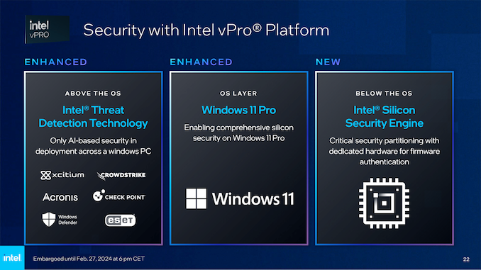
Intel's vPro security features is something we've covered previously – and on that note, Intel has a new Silicon Security Engine giving the chips the ability to authentical the systems firmware. Intel also states that Intel Threat Detection within vPro has been enhanced and adds an additional layer for the NPU, with an xPU model (CPU/GPU/NPU) to help detect a variety of attacks, and also enables 3rd party software to fun faster. Intel claims is the only AI-based security deployment within a Windows PC to date. Both the total Enterprise securities and the cut-down Essentials vPro hardware-level security to select 14th Gen Core series processors, as well as their latest mobile-focused Meteor Lake processors with Arc graphics launched last year.

Intel 14th Gen vPro: Raptor Lake-R Gets Secured

As we've seen over the last few years with a global shift towards remote work due to the Coronavirus pandemic, the need for up-to-date security in small and larger enterprises is just as critical as it has ever been. Remote and employees in offices alike must have access to the latest software and hardware frameworks to ensure the security of vital data, and that's where Intel vPro comes in.

To quickly recap the current state of affairs, let's take a look at the two levels of Intel vPro securities available,  vPro Essentials and vPro Enterprise, and how they differ.

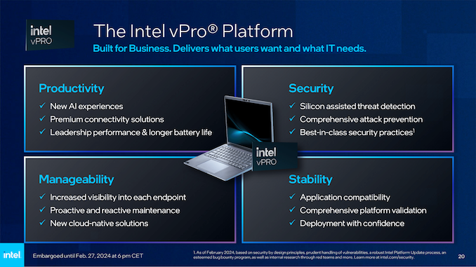
Intel's vPro Essentials was first launched back in 2022 and is a subset of Intel's complete vPro package, which is now commonly known as vPro Enterprise. The Intel vPro Essentials security package is essentially (as per the name) tailored and designed for small businesses, providing a solid foundation in security without penalizing performance. It integrates hardware-enhanced security features, ensuring hardware-level protection against emerging threats from right from its installation. It also utilizes real-time intelligence for workload optimization and Intel's Thread Detection Technology. It adds an additional layer below the operating system that uses AI-based threat detection to mitigate OS-level threats and attacks.

Pivoting to Intel vPro Enterprise security features, this is designed for SMEs to meet the high demands of large-scale business environments. It offers advanced security features and remote management capabilities, which are crucial for businesses operating with sensitive data and requiring high levels of cybersecurity. Additionally, the platform provides enhanced performance and reliability, making it suitable for intensive workloads and multitasking in a professional setting. Integrating these features from the vPro Enterprise platform ensures that large enterprises can maintain high productivity levels while ensuring data security and efficient IT management with the latest generations of processors, such as the Intel Core 14th Gen family.

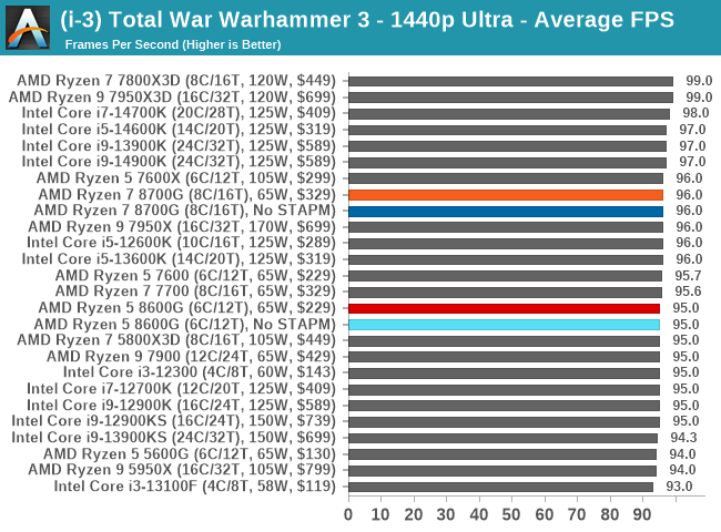
Much like we saw when Intel announced their vPro for the 13th Gen Core series, it's worth noting that both the 14th and 13th Gen Core series are based on the same Raptor Lake architecture and, as such, are identical in every aspect bar base and turbo core frequencies.

Intel 14th Gen Core with vPro for Desktop
(Raptor Lake-R)
AnandTech Cores
P+E/T
P-Core
Base/Turbo
(MHz)
E-Core
Base/Turbo
(MHz)
L3 Cache
(MB)
Base
W
Turbo
W
vPRO
Support
(Ent/Ess)
Price
($)
i9-14900K 8+16/32 3200 / 6000 2400 / 4400 36 125 253 Enterprise $589
i9-14900 8+16/32 2000 / 5600 1500 / 4300 36 65 219 Both $549
i9-14900T 8+16/32 1100 / 5500 800 / 4000 36 35 106 Both $549
 
i7-14700K 8+12/28 3400 / 5600 2500 / 4300 33 125 253 Enterprise $409
i7-14700 8+12/28 2100 / 5400 1500 / 4200 33 65 219 Both $384
i7-14700T 8+12/28 1300 / 5000 900 / 3700 33 35 106 Both $384
 
i5-14600K 6+8/20 3500 / 5300 2600 / 4000 24 125 181 Enterprise $319
i5-14600 6+8/20 2700 / 5200 2000 / 3900 24 65 154 Both $255
i5-14500 6+8/20 2600 / 5000 1900 / 3700 24 65 154 Both $232
i5-14600T 6+8/20 1800 / 5100 1200 / 3600 24 35 92 Both $255
i5-14500T 6+8/20 1700 / 4800 1200 / 3400 24 35 92 Both $232

While Intel isn't technically launching any new chip SKUs (either desktop or mobile) with vPro support, the vPro desktop platform features are enabled through the use of specific motherboard chipsets, with both Q670 and W680 chipsets offering sole support for vPro on 14th Gen. Unless users are using either a Q670 or W680 motherboard with the specific chips listed above. vPro Essentials or Enterprise will not be enabled or work with each processor unless installed into a motherboard from one of these chipsets.

As with the previous 13th Gen Core series family (Raptor Lake), the 14th Gen, which is a direct refresh of these, follows a similar pattern. Specific SKUs from the 14th Gen family include support only for the full-fledged vPro Enterprise, including the Core i5-14600K, the Core i7-14700K, and the flagship Core i9-14900K. Intel's vPro Enterprise security features are supported on both Q670 and W680 motherboards, giving users more choice in which board they opt for.

The rest of the above Intel 14th Gen Core series stack, including the non-monikered chips, e.g., the Core i5-14600, as well as the T series, which are optimized for efficient workloads with a lower TDP than the rest of the stack, all support both vPro Enterprise and vPro Essentials. This includes two processors from the Core i9 family, including the Core i9-14900 and Core i9-14900T, two from the i7 series, the Core i7-14700 and Core i7-14700T, and four from the i5 series, the Core i5-14600, Core i5-14500, the Core i5-14600T and the COre i5-14500T.


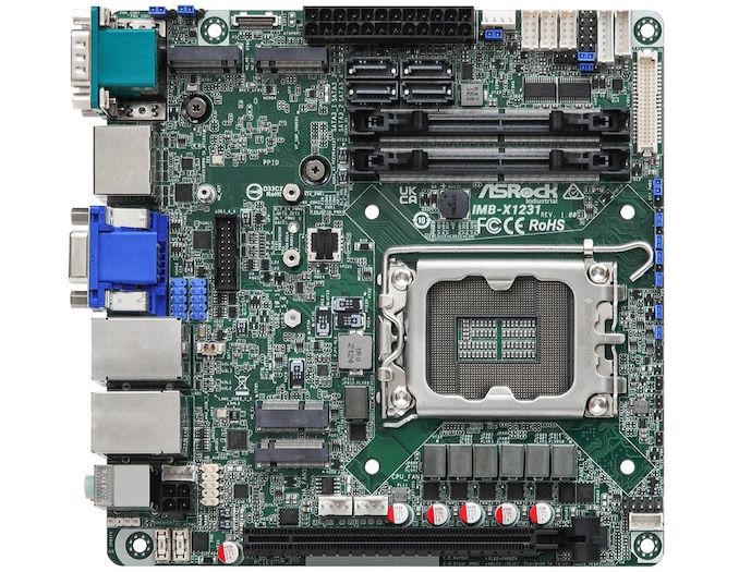
The ASRock Industrial IMB-X1231 W680 mini-ITX motherboard supports vPro Enterprise and Essentials

For the processors mentioned above (non-K), different levels of vPro support are offered depending on the motherboard chipset. If a user wishes to use a Q670 motherboard, then users can specifically opt to use Intel's cut-down vPro Essentials security features. Intel states that users with a Q670 or W680 can use the full vPro Enterprise security features, including the Core i9-14900K, the Core i7-14700K, and the Core i5-14600K. Outside of this, none of the 14th Gen SKUs with the KF (unlocked with no iGPU) and F (no iGPU) monikers are listed with support for vPro.

Intel Meteor Lake with vPro: Core Ultra H and U Series get Varied vPro Support

Further to the Intel 14th Gen Core series for desktops, Intel has also enabled vPro support for their latest Meteor Lake-based Core Ultra H and U series mobile processors. Unlike the desktop platform for vPro, things are a little different in the mobile space, as Intel offers vPro on their mobile SKUs, either with vPro Enterprise or vPro Essentials, not both.

Intel Core Ultra H and U-Series Processors with vPro
(Meteor Lake)
AnandTech Cores
(P+E+LP/T)
P-Core Turbo
Freq
E-Core Turbo
Freq
GPU GPU Freq L3 Cache
(MB)
vPro Support
(Ent/Ess)
Base TDP Turbo TDP
Ultra 9  
Core Ultra 9 185H 6+8+2/22 5100 3800 Arc Xe (8) 2350 24 Enterprise 45 W 115 W
Ultra 7  
Core Ultra 7 165H 6+8+2/22 5000 3800 Arc Xe (8) 2300 24 Enterprise 28 W 64/115 W
Core Ultra 7 155H 6+8+2/22 4800 3800 Arc Xe (8) 2250 24 Essentials 28 W 64/115 W
Core Ultra 7 165U 2+8+2/14 4900 3800 Arc Xe (4) 2000 12 Enterprise 15 W 57 W
Core Ultra 7 164U 2+8+2/14 4800 3800 Arc Xe (4) 1800 12 Enterprise 9 W 30 W
Core Ultra 7 155U 2+8+2/14 4800 3800 Arc Xe (4) 1950 12 Essentials 15 W 57 W
Ultra 5  
Core Ultra 5 135H 4+8+2/18 4600 3600 Arc Xe
(7)
2200 18 Enterprise 28 W 64/115 W
Core Ultra 5 125H 4+8+2/18 4500 3600 Arc Xe (7) 2200 18 Essentials 28 W 64/115 W
Core Ultra 5 135U 2+8+2/14 4400 3600 Arc Xe (4) 1900 12 Enterprise 15 W 57 W
Core Ultra 5 134U 2+8+2/14 4400 3800 Arc Xe (4) 1750 12 Enterprise 9 W 30 W
Core Ultra 5 125U 2+8+2/14 4300 3600 Arc Xe (4) 1850 12 Essentials 15 W 57 W

The above table highlights not just the specifications of each Core Ultra 9, 7, and 5 SKU but also denotes which model gets what level of vPro support. Starting with the Core Ultra 9 185H processor, the current mobile flagship chip on Meteor Lake, this chip supports vPro Enterprise. Along with the other top-tier SKU from each of the Core Ultra 9, 7, and 5 families, including the Core Ultra 7 165H and the Core Ultra 135H, other chips with vPro Enterprise support include the Core Ultra 7 165U and Core Ultra 7 164U, as well as the Core Ultra 5 135U and Core Ultra 5 134U.

Intel's other Meteor Lake chips, including the Core Ultra 7 155H, the Core Ultra 7 155U, the Core Ultra 5 125H, and the Core Ultra 5 125U, only come with support Intel's vPro Essentials features and not with support for Enterprise This presents a slight 'dropping of the ball' from Intel on this, which we highlighted in our Intel 13th Gen Core gets vPro piece last year.

Intel vPro Support Announcement With No New Hardware, Why Announce Later?

It is worth noting that Intel's announcement of adding vPro support to their first launch of Meteor Lake Core Ultra SKUs isn't entirely new; Intel did highlight that Meteor Lake would support vPro last year within their Series 1 Product Brief dated 12/20/2023. Intel's formal announcement of vPro support for Meteor Lake is more about which SKU has which level of support, and we feel this could pose problems to users who have already purchased Core Ultra series notebooks for business and enterprise use. Multiple outlets, including Newegg and directly from HP, are alluding to mentioning vPro whatsoever.

This could mean that a user has purchased a notebook with, say, a Core Ultra 5 125H (vPro Essentials), which would be used within an SME or by said SME as a bulk purchase but wouldn't be aware that the chip doesn't have vPro Enterprise, from which they personally and from a business standpoint could benefit from the additional securities. We reached out to Intel, and they sent us the following statement.

"Since we are launching vPro powered by Intel Core Ultra & Intel Core 14th Gen this week, prospective buyers will begin seeing the relevant system information on OEM and enterprise retail partner (eg. CDW) websites in the weeks ahead. This will include information on whether a system is equipped with vPro Enterprise or Essentials so that they can purchase the right system for their compute needs."

Tenstorrent Licenses RISC-V CPU IP to Build 2nm AI Accelerator for Edge

Tenstorrent this week announced that it had signed a deal to license out its RISC-V CPU and AI processor IP to Japan's Leading-edge Semiconductor Technology Center (LSTC), which will use the technology to build its edge-focused AI accelerator. The most curious part of the announcement is that this accelerator will rely on a multi-chiplet design and the chiplets will be made by Japan's Rapidus on its 2nm fabrication process, and then will be packaged by the same company.

Under the terms of the agreement, Tenstorrent will license its datacenter-grade Ascalon general-purpose processor IP to LSTC and will help to implement the chiplet using Rapidus's 2nm fabrication process. Tenstorrent's Ascalon is a high-performance out-of-order RISC-V CPU design that features an eight-wide decoding. The Ascalon core packs six ALUs, two FPUs, and two 256-bit vector units and when combined with a 2nm-class process technology promises to offer quite formidable performance.

The Ascalon was developed by a team led by legendary CPU designer Jim Keller, the current chief executive of Tenstorrent, who used to work on successful projects by AMD, Apple, Intel, and Tesla.

In addition to general-purpose CPU IP licensing, Tenstorrent will co-design 'the chip that will redefine AI performance in Japan.' This apparently means that Tenstorrent  does not plan to license LSTC its proprietary  Tensix cores tailored for neural network inference and training, but will help to design a proprietary AI accelerator generally for inference workloads.

"The joint effort by Tenstorrent and LSTC to create a chiplet-based edge AI accelerator represents a groundbreaking venture into the first cross-organizational chiplet development in semiconductor industry," said Wei-Han Lien, Chief Architect of Tenstorrent's RISC-V products. "The edge AI accelerator will incorporate LSTC's AI chiplet along with Tenstorrent's RISC-V and peripheral chiplet technology. This pioneering strategy harnesses the collective capabilities of both organizations to use the adaptable and efficient nature of chiplet technology to meet the increasing needs of AI applications at the edge."

Rapidus aims to start production of chips on its 2nm fabrication process that is currently under development sometimes in 2027, at least a year behind TSMC and a couple of years behind Intel. Yet, if it starts high-volume 2nm manufacturing in 2027, it will be a major breakthrough from Japan, which is trying hard to return to the global semiconductor leaders.

Building an edge AI accelerator based on Tenstorrent's IP and Rapidus's 2nm-class production node is a big deal for LSTC, Tenstorrent, and Rapidus as it is a testament for technologies developed by these three companies.

"I am very pleased that this collaboration started as an actual project from the MOC conclusion with Tenstorrent last November," said Atsuyoshi Koike, president and CEO of Rapidus Corporation. "We will cooperate not only in the front-end process but also in the chiplet (back-end process), and work on as a leading example of our business model that realizes everything from design to back-end process in a shorter period of time ever."

The Cooler Master MWE V2 Gold 750W PSU Review: Effective, But Limited By Aging Platform

Cooler Master, renowned for its pioneering role in cooling technologies, has evolved into a key player in the PC components industry, extending its expertise to include cases and power supply units (PSUs). The company's current catalog is a testament to its commitment to diversity, featuring over 75 PC cases, 90 coolers, and 120 PSUs, all designed to cater to the evolving demands of tech enthusiasts and professionals alike.

This review focuses on the Cooler Master MWE Gold V2 750W PSU, a key offering in Cooler Master's power supply lineup that embodies the brand's vision of combining quality and value. The MWE Gold V2 series is engineered to offer solid performance and reliability at a price point that appeals to system builders and gamers looking for an entry-level to mid-range solution. As a result, the MWE Gold V2 750W has been a consistently popular offering within Cooler Master's catalog, often cycling in and out of stock depending on what sales are going on. This makes the PSU a bit harder to track down in North America than it does Europe, and quick to vanish when it does show up.

SK Hynix Mulls 'Differentiated' HBM Memory Amid AI Frenzy

SK Hynix and AMD were at the forefront of the memory industry with the first generation of high bandwidth memory (HBM) back in 2013 – 2015, and SK Hynix is still leading this market in terms of share. In a bid to maintain and grow its position, SK Hynix has to adapt to the requirements of its customers, particularly in the AI space, and to do so it's mulling over how to make 'differentiated' HBM products for large customers.

"Developing customer-specific AI memory requires a new approach as the flexibility and scalability of the technology becomes critical," said Hoyoung Son, the head of Advanced Package Development at SK Hynix in the status of a vice president

When it comes to performance, HBM memory with a 1024-bit interface has been evolving fairly fast: it started with a data transfer rate of 1 GT/s in 2014 – 2015 and reached upwards of 9.2 GT/s – 10 GT/s with the recently introduced HBM3E memory devices. With HBM4, the memory is set to transit to a 2048-bit interface, which will ensure steady bandwidth improvement over HBM3E.

But there are customers which may benefit from differentiated (or semi-custom) HBM-based solutions, according to the vice president.

"For implementing diverse AI, the characteristics of AI memory also need to become more varied," Hoyoung Son said in an interview with BusinessKorea. "Our goal is to have a variety of advanced packaging technologies capable of responding to these changes. We plan to provide differentiated solutions that can meet any customer needs."

With a 2048-bit interface, many (if not the vast majority) of HBM4 solutions will likely be custom or at least semi-custom based on what we know from official and unofficial information about the upcoming standard. Some customers might want to keep using interposers (but this time they are going to get very expensive) and others will prefer to install HBM4 modules directly on logic dies using direct bonding techniques, which are also expensive.

Making differentiated HBM offerings requires sophisticated packaging techniques, including (but certainly not limited to) SK Hynix's Advanced Mass Reflow Molded Underfill (MR-RUF) technology. Given the company's vast experience with HBM, it may well come up with something else, especially for differentiated offerings.

"For different types of AI to be realized, the characteristics of AI memory also need to be more diverse," the VP said. "Our goal is to have a range of advanced packaging technologies to respond to the shifting technological landscape. Looking ahead, we plan to provide differentiated solutions to meet all customer needs."

Sources: BusinessKorea, SK Hynix

Silicon Power PX10 Portable SSD Review: One Step Forward, Two Steps Back

Silicon Power announced the MS70 and PX10 Portable SSDs in late 2023. The company is well known for offering entry- and mid-range products at compelling price points, but the two products came with plenty of promises in the 1GBps-class category. The MS70 promised high storage density (up to 2TB in a compact thumb drive), while the PX10 targeted power users and professionals with performance consistency as the focus. Read on for a detailed look at the Silicon Power PX10 including an analysis of its internals, value proposition, and evaluation of its performance consistency, power consumption, and thermal profile.

Apple Launches M3-Based MacBook Air 13 and 15: 3nm CPU for the Masses

Apple on Monday introduced its new generation MacBook Air laptops based on the company's most-recent M3 system-on-chip (SoC). The new MacBook Air notebooks come in the same sizes as the previous models – 13.6 inches and 15.3 inches – with prices starting from $1,099 and $1,299 respectively.

The key improvement in Apple's 2024 MacBook Air laptops is of course the M3 processor. Fabbed on TSMC's N3B process, Apple's latest mainstream SoC was first launched late last year as part of the 2023 MacBook Pro lineup, and is now being brought down to the MacBook Air family. The vanilla M3 features four high-performance cores operating at up to 4.05 GHz, four energy-efficient cores, a 10 core GPU based on the latest graphics architecture (with dynamic caching, hardware-accelerated ray tracing, and hardware-accelerated mesh shading), and a new media engine with hardware-accelerated AV1 decoding.

MacBook Air Specifications
Model MBA 15
2024
MBA 13
2024
MBA 15
2023
MBA 13
2022
MBA 13
2020
CPU Apple M3
4C/4T High-Perf + 4C/4T High-Eff
Apple M2
4C/4T High-Perf + 4C/4T High-Eff
Apple M1
4C/4T High-Perf +
4C/4T High-Eff
GPU Apple M3 Integrated
(8 or 10 Cores)
Apple M2 Integrated
(8 or 10 Cores)
Apple M1 Integrated
(7 or 8 Cores)
Memory 8 - 24 GB LPDDR5-6400 8 - 24 GB LPDDR5-6400 8 - 16 GB LPDDR4X-4266
SSD 256 GB - 2 TB 256 GB - 2 TB 256 GB - 2 TB
I/O 2x USB4 Type-C
w/Thunderbolt 3
1x MagSafe 3
3.5mm Audio
Touch ID
2x USB4 Type-C
w/Thunderbolt 3
1x MagSafe 3
3.5mm Audio
Touch ID
2x USB4 Type-C
w/Thunderbolt 3

3.5mm Audio
Touch ID
Display 15.3-inch 2880x1864 IPS LCD
P3 with True Tone
13.6-inch 2560x1664 IPS LCD
P3 with True Tone
15.3-inch 2880x1864 IPS LCD
P3 with True Tone
13.6-inch 2560x1664 IPS LCD
P3 with True Tone
13.3-inch 2560x1600 IPS LCD
P3 with True Tone
Dimensions Width 34.0 cm 30.4 cm 34.0 cm 30.4 cm 30.4 cm
Depth 23.7 cm 21.5 cm 23.7 cm 21.5 cm 21.2 cm
Height 1.1 cm 1.1 cm 1.1 cm 1.1 cm 0.41 - 1.61 cm
Weight 3.3 lbs (1.5 kg) 2.7 lbs (1.22 kg) 3.3 lbs (1.5 kg) 2.7 lbs (1.22 kg) 2.8 lbs (1.29 kg)
Battery Capacity 66.5 Wh 52.6 Wh 66.5 Wh 52.6 Wh 49.9 Wh
Battery Life 15 - 18 Hours 15 - 18 Hours 15 - 18 Hours
Price $1299 $1099 $1299 $1199 $999

Like prior vanilla M-series SoC, the M3 offers two display engines, allowing it to drive up to two displays. Normally this has been one internal and one external display, but new to the M3/2024 MBAs, the laptop can also drive two external 5K displays when the internal display is disabled (e.g. the lid's closed).

With regards to performance, Apple is opting to compare the new AIrs to the 2020 models with Apple's M1 SoC. The CPU is said to be up to 35% – 60% faster compared to the original M1 chip depending on the workload, but such comparisons should be taken with a grain of salt as companies tend to overhype their biggest advantages. One thing to keep in mind is that since MacBook Airs come without active cooling, their performance is typically lower than MacBook Pros running the same processor.

The SoC supports up to 24 GB of LPDDR5-6400 memory (featuring bandwidth of 100 GB/s), though entry-level MacBook Air models still feature only a diminutive 8 GB of RAM and a 256 GB SSD. More advanced (and usable) configurations offer 16 GB or 24 GB of memory and up to 2 TB of solid-state storage.

Other improvements of Apple's 2024 MacBook Air laptops based on the M3 processor compared to predecessors include Wi-Fi 6E support;  improved three-microphones array with enhanced voice clarity, voice isolation, and wide spectrum modes.

As for input/output capabilities, the new MacBook Air notebooks feature two Thunderbolt 4/USB-C ports, a MagSafe port for charging, a 3.5-mm jack for headsets, and a 1080p FaceTime HD camera.

The 2024 Apple MacBook Air come in midnight, starlight, silver, and space gray colors. The machines are equipped with a 52.6 Wh battery that provides up to 18 hours of video playback. The 13.6-inch machine is 0.44 inch (1.13 cm) thick and weighs 2.7 pounds (1.24 kilograms), whereas the 15.3-inch laptop is 0.45 inch (1.15 cm) thick and weighs 3.3 pounds (1.51 kilograms).

With the launch of its M3-based MacBook Airs, Apple will discontinue its M2-based MacBook Air 15, but will retain the M2-based MacBook Air 13 as their entry-level option, with prices now starting at $999.

JEDEC Publishes GDDR7 Memory Spec: Next-Gen Graphics Memory Adds Faster PAM3 Signaling & On-Die ECC

JEDEC on Tuesday published the official specifications for GDDR7 DRAM, the latest iteration of the long-standing memory standard for graphics cards and other GPU-powered devices. The newest generation of GDDR brings a combination of memory capacity and memory bandwidth gains, with the later being driven primarily by the switch to PAM3 signaling on the memory bus. The latest graphics RAM standard also boosts the number of channels per DRAM chip, adds new interface training patterns, and brings in on-die ECC to maintain the effective reliability of the memory.

“JESD239 GDDR7 marks a substantial advancement in high-speed memory design,” said Mian Quddus, JEDEC Board of Directors Chairman. “With the shift to PAM3 signaling, the memory industry has a new path to extend the performance of GDDR devices and drive the ongoing evolution of graphics and various high-performance applications.”

GDDR7 has been in development for a few years now, with JEDEC members making the first disclosures around the memory technology about a year ago, when Cadence revealed the use of PAM3 encoding as part of their validation tools. Since then we've heard from multiple memory manufacturers that we should expect the final version of the memory to launch in 2024, with JEDEC's announcement essentially coming right on schedule.

As previously revealed, the biggest technical change with GDDR7 comes with the switch from two-bit non-return-to-zero (NRZ) encoding on the memory bus to three-bit pulse amplitude modulating (PAM3) encoding. This change allows GDDR7 to transmit 3 bits over two cycles, 50% more data than GDDR6 operating at an identical clockspeed. As a result, GDDR7 can support higher overall data transfer rates, the critical component to making each generation of GDDR successively faster than its predecessor.

GDDR Generations
  GDDR7 GDDR6X
(Non-JEDEC)
GDDR6
B/W Per Pin 32 Gbps (Gen 1)
48 Gbps (Spec Max)
24 Gbps (Shipping) 24 Gbps (Sampling)
Chip Density 2 GB (16 Gb) 2 GB (16 Gb) 2 GB (16 Gb)
Total B/W (256-bit bus) 1024 GB/sec 768 GB/sec 768 GB/sec
DRAM Voltage 1.2 V 1.35 V 1.35 V
Data Rate QDR QDR QDR
Signaling PAM-3 PAM-4 NRZ (Binary)
Maximum Density 64 Gb 32 Gb 32 Gb
Packaging 266 FBGA 180 FBGA 180 FBGA

The first generation of GDDR7 is expected to run at data rates around 32 Gbps per pin, and memory manufacturers have previously talked about rates up to 36 Gbps/pin as being easily attainable. However the GDDR7 standard itself leaves room for even higher data rates – up to 48 Gbps/pin – with JEDEC going so far as touting GDDR7 memory chips "reaching up to 192 GB/s [32b @ 48Gbps] per device" in their press release. Notably, this is a significantly higher increase in bandwidth than what PAM3 signaling brings on its own, which means there are multiple levels of enhancements within GDDR7's design.

Digging deeper into the specification, JEDEC has also once again subdivided a single 32-bit GDDR memory chip into a larger number of channels. Whereas GDDR6 offered two 16-bit channels, GDDR7 expands this to four 8-bit channels. The distinction is somewhat arbitrary from an end-user's point of view – it's still a 32-bit chip operating at 32Gbps/pin regardless – but it has a great deal of impact on how the chip works internally. Especially as JEDEC has kept the 256-bit per channel prefetch of GDDR5 and GDDR6, making GDDR7 a 32n prefetch design.


GDDR Channel Architecture. Original GDDR6-era Diagram Courtesy Micron

The net impact of all of this is that, by halving the channel width but keeping the prefetch size the same, JEDEC has effectively doubled the amount of data that is prefetched per cycle of the DRAM cells. This is a pretty standard trick to extend the bandwidth of DRAM memory, and is essentially the same thing JEDEC did with GDDR6 in 2018. But it serves as a reminder that DRAM cells are still very slow (on the order of hundreds of MHz) and aren't getting any faster. So the only way to feed faster memory buses is by fetching ever-larger amounts of data in a single go.

The change in the number of channels per memory chip also has a minor impact on how multi-channel "clamshell" mode works for higher capacity memory configurations. Whereas GDDR6 accessed a single memory channel from each chip in a clamshell configuration, GDDR7 will access two channels – what JEDEC is calling two-channel mode. Specifically, this mode reads channels A and C from each chip. It is effectively identical to how clamshell mode behaved with GDDR6, and it means that while clamshell configurations remain supported in this latest generation of memory, there aren't any other tricks being employed to improve memory capacity beyond ever-increasing memory chip densities.

On that note, the GDDR7 standard officially adds support for 64Gbit DRAM devices, twice the 32Gbit max capacity of GDDR6/GDDR6X. Non-power-of-two capacities continue to be supported as well, allowing for 24Gbit and 48Gbit chips. Support for larger memory chips further pushes the maximum memory capacity of a theoretical high-end video card with a 384-bit memory bus to as high as 192GB of memory – a development that would no doubt be welcomed by datacenter operators in the era of large language AI models. With that said, however, we're still regularly seeing 16Gbit memory chips used on today's memory cards, even though GDDR6 supports 32Gbit chips. Coupled with the fact that Samsung and Micron have already disclosed that their first generation of GDDR7 chips will also top out at 16Gbit/24Gbit respectively, it's safe to say that 64Gbit chips are pretty far off in the future right now (so don't sell off your 48GB cards quite yet).

For their latest generation of memory technology, JEDEC is also including several new-to-GDDR memory reliability features. Most notably, on-die ECC capabilities, similar to what we saw with the introduction of DDR5. And while we haven't been able to get an official comment from JEDEC on why they've opted to include ECC support now, its inclusion is not surprising given the reliability requirements for DDR5. In short, as memory chip densities have increased, it has become increasingly hard to yield a "perfect" die with no flaws; so adding on-chip ECC allows memory manufacturers to keep their chips operating reliably in the face of unavoidable errors.


This figure is reproduced, with permission, from JEDEC document JESD239, figure 124

Internally, the GDDR7 spec requires a minimum of 16 bits of parity data per 256 bits of user data (6.25%), with JEDEC giving an example implementation of a 9-bit single error correcting code (SEC) plus a 7-bit cyclic redundancy check (CRC). Overall, GDDR7 on-die ECC should be able to correct 100% of 1-bit errors, and detect 100% of 2-bit errors – falling to 99.3% in the rare case of 3-bit errors. Information about memory errors is also made available to the memory controller, via what JEDEC terms their on-die ECC transparency protocol. And while technically separate from ECC itself, GDDR7 also throws in another memory reliability feature with command address parity with command blocking (CAPARBLK), which is intended to improve the integrity of the command address bus.

Otherwise, while the inclusion of on-die ECC isn't likely to have any more of an impact on consumer video cards than its inclusion had for DDR5 memory and consumer platforms there, it remains to be seen what this will mean for workstation and server video cards. The vendors there have used soft ECC on top of unprotected memory for several generations now; presumably this will remain the case for GDDR7 cards as well, but the regular use of soft ECC makes things a lot more flexible than in the CPU space.


This figure is reproduced, with permission, from JEDEC document JESD239, figure 152

Finally, GDDR7 is also introducing a suite of other reliability-related features, primarily related to helping PAM3 operation. This includes core independent LFSR (linear-feedback shift register) training patterns with eye masking and error counters. LFSR training patterns are used to test and adjust the interface (to ensure efficiency), eye masking evaluates signal quality, and error counters track the number of errors during training.

Technical matters aside, this week's announcement includes statements of support from all of the usual players on both sides of the isle, including AMD and NVIDA, and the Micron/Samsung/SKhynix trifecta. It goes without saying that all parties are keen to getting to use or sell GDDR7 respectively, given the memory capacity and bandwidth improvements it will bring – and especially in this era where anything aimed at the AI market is selling like hotcakes.

No specific products are being announced at this time, but with Samsung and Micron having previously announced their intentions to ship GDDR7 memory this year, we should see new memory (and new GPUs to pair it with) later this year.

JEDEC standards and publications are copyrighted by the JEDEC Solid State Technology Association.  All rights reserved.

Western Digital Issues Update on Company Split: CEOs for Post-Split Entities Announced

Now well in the midst of executing its plan to divide itself into separate hard drive and NAND businesses, Western Digital today offered a fresh update on the state of that split, and what the next steps are for the company. With the eventual goal of dividing the company into two independent, publicly traded companies, Western Digital is reporting that they have made significant progress in key transactional projects, and they are also announcing their initial leadership appointments for the post-separation businesses.

Western Digital's separation, announced on October 30, 2023, aims to create two focused companies with distinct product lineups for hard drives and NAND flash memory, respectively, as well as NAND flash memory-based products. This move is expected to speed up innovation and introduce new growth opportunities, according to Western Digital. Meanwhile, with separate capital structures, operational efficiency of the two entities will be higher compared to the united company, the management of Western Digital claims.

Western Digital led the storage industry's consolidation by acquiring HGST, various SSD and flash companies in the early 2010s, and SanDisk in 2016 for NAND flash production. As a result, in late 2010s the company become a media-agnostic, vertically-integrated storage technology company. However, the company faced challenges in growing its revenue. The 3D NAND and SSD markets are highly competitive commodity markets, and as a result they tend to fluctate depending on supply and demand. Meanwhile, demand for HDDs is declining and offseting decreasing unit sales with 3D NAND-based products and nearline hard drives was challenging. Meanwhile, to avoid avoid competition with larger storage solutions providers like Dell, HPE, and IBM — which purchase Western Digital's HDDs, SSDs, and NAND memory — Western Digital had to divest its storage solutions, which presents additional challenges.

As a result, Western Digital's HDD and NAND businesses have acted largely independently since late 2020, when it became apparent that the combined company has failed to become bigger than the sum of Western Digital and SanDisk parts. So far, quite some progress has been made in preparing for the separation, including establishing legal entities in 18 countries, preparing independent financial models, and finalizing preparations for regulatory filings. As a result, the company remains on track to finish the split in the second-half of this year, according to Western Digital.

With regards to post-split leadership, David Goeckeler has been appointed as the chief executive designate for the NAND flash memory spinoff company. He expressed enthusiasm for the NAND business's potential in market growth and the development of new memory technologies.

"Today's announcement highlights the important steps we are making towards the completion of an extremely complex transaction that incorporates over a dozen countries and spans data storage technology brands for consumers to professional content creators to the world’s leading device OEMs and the largest cloud providers," said David Goeckeler, CEO of Western Digital. "I am pleased with the exceptional work the separation teams have done so far in creating a spin-ready foundation that will ensure a successful transition to independent, market-leading companies for our Flash and HDD businesses."

Meanwhile, Irving Tan, currently executive vice president of global operations, will assume the CEO role for the standalone HDD company, which will continue to operate under the Western Digital brand. It is unclear where Ashley Gorakhpurwalla, currently the head of WDC's HDD business unit, will end up, or if he'll even remain with the company at all.

"While both Western Digital's businesses will have the strategic focus and resources to pursue exciting opportunities in their respective markets once the separation is complete, the Flash business offers exciting possibilities with market growth potential and the emerging development of disruptive, new memory technologies," added Goeckeler. "I am definitely looking forward to what's next for the spinoff team."

SanDisk Professional PRO-BLADE Portable SSD Ecosystem Review

Western Digital had unveiled the SanDisk Professional PRO-BLADE modular SSD ecosystem in mid-2022 to serve the needs of the professional market. Compact and sturdy NVMe drives (PRO-BLADE SSD Mag) swappable across discrete bus-powered enclosures (PRO-BLADE TRANSPORT), and also compatible with a multi-bay reader (PRO-BLADE STATION) have perfectly fit the requirements of multi-user / multi-site workflows in the content capture industry. Read on for a detailed look at the first-generation PRO-BLADE SSD Mags and the PRO-BLADE TRANSPORT enclosure. In addition to the evaluation of the performance consistency, power consumption, and thermal profile, an analysis of the internals is also included.

❌