Vue normale

Il y a de nouveaux articles disponibles, cliquez pour rafraîchir la page.
Aujourd’hui — 5 juin 2024AnandTech

G.Skill Demonstrates DDR5-10600 Memory Modules On Ryzen 8500G System

5 juin 2024 à 14:30

Ultra-high performance memory modules are a staple of of Computex, and it looks like this year G.Skill is showing off the highest performance dual-channel memory module kit to date. The company is demonstrating a DDR5 kit capable of 10,600 MT/s data transfer rate, which is a considerably higher speed compared to memory modules available today.

The dual-channel kit that G.Skill is demonstrating is a 32 GB Trident Z5 RGB kit that uses cherry-picked DDR5 memory devices and which can work in a DDR5-10600 mode with CL56 62-62-126 timings at voltages that are way higher than standard. The demoed DIMMs are running the whole day in a fairly warm room, though it does not really run demanding applications or stress tests.

Traditionally, memory module makers like G.Skill use Intel processors to demonstrate their highest-performing kits. But with the DDR5-10600 kit, the company uses AMD's Ryzen 5 8500G processor, which is a monolithic Zen 4-based APU with integrated graphics that's normally sold for budget systems. The motherboard is a high-end Asus ROG Crosshair X670E Gene and the APU is cooled down using a custom liquid cooling system The Asus ROG Crosshair X670E Gene motherboard has only two memory slots, which greatly helps to enable high data transfer rates, so it is a very good fit for the DDR5-10600 dual-channel kit.

Though I have sincere doubts that someone is going to use an ultra-expensive DDR5-10600 memory kit and related gate with this inexpensive processor, it is interesting (and unexpected) to see an AMD APU as a good fit to demonstrate performance potential of G.Skill's upcoming modules.

Speaking of availability of G.Skill's DDR5-10600 memory, it does not look like this kit is around the corner. The fastest DDR5 kit that G.Skill has today is its DDR5-8400 offering, so the DDR5-10600 will come to market a few speed bins later as G.Skill certainly needs to test the kit with various CPUs and ensure its stability. 

One other thing to keep in mind is that both AMD and Intel are about to release new desktop processors this year, with the Ryzen 9000-series and Arrow Lake processors respectively. So G.Skill will undoubtedly focus on tuning its DDR5-10600 and other high-end kits primarily with those new CPUs.

Update on Intel's Panther Lake at Computex 2024, Intel Powering Up Intel 18A Wafer Next Week

5 juin 2024 à 03:00

During the Intel keynote hosted by CEO Pat Gelsinger, he gave the world a glimpse into the Intel Client roadmap until 2026. Meteor Lake launched last year on that roadmap, and Lunar Lake, which we dived into yesterday as Intel disclosed technical details about the upcoming platform. Pat also presented a wafer on stage, Panther Lake, and he gave some additional information about Intel's forthcoming Panther Lake platform, which is expected in 2025.

We covered Intel's initial announcement about the Panther Lake platform last year. It is set to be Intel's first client platform using its Intel 18A node. Aside from once again affirming that things are on track for a 2026 launch, Pat Gelsinger, Intel's CEO, also confirmed that they will be powering on the first 18A wafer for Panther Lake as early as next week.

Intel CPU Architecture Generations
  Alder/Raptor Lake Meteor
Lake
Lunar
Lake
Arrow
Lake
Panther
Lake
P-Core Architecture Golden Cove/
Raptor Cove
Redwood Cove Lion Cove Lion Cove Cougar Cove?
E-Core Architecture Gracemont Crestmont Skymont Crestmont? Darkmont?
GPU Architecture Xe-LP Xe-LPG Xe2 Xe2? ?
NPU Architecture N/A NPU 3720 NPU 4 ? ?
Active Tiles 1 (Monolithic) 4 2 4? ?
Manufacturing Processes Intel 7 Intel 4 + TSMC N6 + TSMC N5 TSMC N3B + TSMC N6 Intel 20A + More Intel 18A + ?
Segment Mobile + Desktop Mobile LP Mobile HP Mobile + Desktop Mobile?
Release Date (OEM) Q4'2021 Q4'2023 Q3'2024 Q4'2024 2025

One element to consider from last year is that Lunar Lake is built using TSMC, with the Lunar Lake compute tile with Xe2-LPG graphics on TSMC N3B, and the I/O tile on TSMC N6. Pat confirmed on stage that Panther Lake will be on Intel 18A. Still, he didn't confirm whether the chip will be made purely at Intel, or a mix between Intel and external foundries (ala Meteor Lake). Intel has also yet to confirm the CPU cores to be used, but from what our sources tell us, it sounds like it will be the new Cougar Cove and Darkmont cores.

As we head into the second half of 2024 and after Lunar Lake launches, Intel may divulge more information, including the architectural advancements Panther Lake is expected to bring. Until then, we will have to wait and see.

Hier — 4 juin 2024AnandTech

Frore Demos Solid-State AirJet Cooler in Action: Significantly Improving Both Laptop and SSD Performance

4 juin 2024 à 22:00

In recent months, Frore Systems has been turning heads with their fanless solid-state air cooler technology. The AirJet, as it's come to be called, was previously shown off at CES this year; and for Computex, the company is back with a fresh round of demonstrations.

For the show, Frore has a number of demonstrations running in a fairly large showroom. The company is looking to address a wide range of products, from tablets to notebooks to small PCs, as well as embedded tablets. But there were two showcases in particular that caught my immediate attention: a Samsung Galaxy Book with and without Frore's AirJet, and an 8 TB Sabrent SSD in an external enclosure.

The Samsung Galaxy Book 2 Pro is an ultra-thin notebook that is normally cooled by a fan that, as argued by Flore, does not do its job properly. According to the company, the stock laptop only has enough cooling capacity to sustain 12W heat/power before it hits Tmax, whereas a retrofitted version with Frore's AirJet installed allows it to hold steady-state operation at 16W – and consequently delivering higher performance. In terms of Cinebench R23 multi-threaded results, we are talking about 5330 points for the modded notebook, versus 4255 for the off-the-shelf Galaxy Book 2 Pro.

The potential use cases for Frore Systems's AirJet solid-state cooling technology do not end with CPUs, either. As mentioned previously, the company is also demonstrating the AirJet Mini on Sabrent 8TB SSDs in Orico external enclosures, showcasing the advantage of the silent active cooler over passive cooling. The passively-cooled drive reached 62°C and leveled out at 1,320 MB/s due to thermal throttling. In contrast, the AirJet-cooled drive maintained a temperature of 42°C and achieved a considerably higher performance of 3,016 MB/s.

According to Frore, this significant improvement in both temperature and performance has already led to one major external SSD vendor adopting AirJet technology to improve the performance of their drives. Unfortunately, Frore isn't naming any names, only stating that it's a "big name."

Now, Frore's AirJet Mini and Mini Slim coolers can dissipate up to 5W of power each, and can be combined in to larger blocks of up to 5 coolers (we are talking about announced solutions, technologically scaling could he higher, but this is an entirely different conversation). So the technology does have some scalability limitations that makes it best-suited for lower-power devices. None the less, removing 25W of thermal energy from a modern laptop without a fan can make a huge difference in the performance of these normally passively-cooled devices.

Of course, the main goal for these Computex demos is far more than just showing off AirJets to the public; what Frore would really like to do is to land a deal for its solid-state cooling solution with a major PC vendor (e.g., Apple, Samsung, etc.). Though to do that, Frore has to pass qualification tests and ensure availability of its products, which is something the company says it's currently working on. Meanwhile, from performance point of view, especially given their dimensions, AirJets look very impressive.

Intel Unveils Lunar Lake Architecture: New P and E cores, Xe2-LPG Graphics, New NPU 4 Brings More AI Performance

4 juin 2024 à 03:00

Intel this morning is lifting the lid on some of the finer architectural and technical details about its upcoming Lunar Lake SoC – the chip that will be the next generation of Core Ultra mobile processors. Once again holding one of their increasingly regular Tech Tour events for media and analysts, Intel this time set up shop in Taipei just before the beginning of Computex 2024. During the Tech Tour, Intel disclosed numerous facets of Lunar Lake, including their new P-Core design codenamed Lion Cove and a new wave of E-cores that are a bit more like Meteor Lake's pioneering Low Power Island E-Cores. Also disclosed was the Intel NPU 4, which Intel claims delivers up to 48 TOPS, surpassing Microsoft's Copilot+ requirements for the new age of AI PCs.

Intel's Lunar Lake represents a strategic evolution in their mobile SoC lineup, building on their Meteor Lake launch last year, focusing on enhancing power efficiency and optimizing performance across the board. Lunar Lake dynamically allocates tasks to efficient cores (E-cores) or performance cores (P-cores) based on workload demands by leveraging advanced scheduling mechanisms, which are assigned to ensure optimal power usage and performance. Still, once again, Intel Thread Director, along with Windows 11, plays a pivotal role in this process, guiding the OS scheduler to make real-time adjustments that balance efficiency with computational power depending on the intensity of the workload.

The Intel Computex 2024 Keynote Live Blog (8:00pm PT/03:00 UTC)

4 juin 2024 à 02:00

Closing out the last of the major PC-focused keynotes at Computex 2024 this evening, we have Intel. The long-reigning leader of the PC CPU market, Intel is in the middle of executing its plans to get back on track on both the manufacturing and chip design aspects of the business. Tonight’s keynote, being helmed by the highly-animated Pat Gelsinger, is titled “Bringing AI Everywhere.” And, like so many other Computex presentations and announcements this week, AI hardware is going to play a big part, as Intel outlines a full stack of products for client and server computing.

Of the four great PC chip vendors at the show, Intel has been the most up-front about what to expect from their hour-long presentation. The company’s Computex 2024 page already outlines their four major topics: AI PCs, Xeon 6 Processors, Gaudi AI accelerators, and Intel’s OpenVINO software ecosystem.

On the consumer hardware front, the company set the table with a significant teaser earlier this month about their forthcoming mobile PC SoC, Lunar Lake. The next generation of Core Ultra processors, Intel is touting significant energy efficiency gains for the mobile-focused chip, with new architectures driving their Performance and Efficiency CPU cores, Xe2 GPU, and a much faster 45+ TOPS (INT8) NPU. While the Lunar Lake announcement is coming relatively soon after the Meteor Lake launch, Intel has made it clear that it’s not going to hold back on shipping future products; they are looking to make up for lost time. Still, Lunar Lake devices are not expected to hit retail shelves until Q4 of this year, so this announcement is coming months in advance of the hardware itself.

On the server front, Intel has been publicly prepping for the launch of a new generation of Xeons with the Xeon 6 platform. The most notable part of this being the release of the company’s first Efficiency-core Xeon, Sierra Forest. Sierra Forest is set to be the first Xeon 6 chip out the door this year, and will offer up to 288 E cores on a single chip, allowing Intel to tap into the many (many) core CPU markets that AMD and Arm-based rivals have been unopposed at thus far.

Finally, the company has fully pivoted its server AI accelerator strategy to its Gaudi accelerators. Gaudi 3 was introduced back in April, and while it isn’t expected to go toe-to-toe with NVIDIA’s top accelerators in every workload, Intel is betting that they can beat NVIDIA on critical workloads, all while undercutting them significantly in pricing. The first Gaudi 3 parts are set to be released in the second half of this year, so hopefully we’ll be hearing a bit more about Intel’s plans as part of their keynote.

As always, the AnandTech crew is live and in person to catch this final Computex keynote. So please come join us at 8:00pm PT / 11:00pm ET / 03:00 UTC to get all the details.

À partir d’avant-hierAnandTech

AMD Announces Zen 5-based EPYC “Turin” Processors: Up to 192 Cores, Coming in H2’2024

3 juin 2024 à 17:15

With AMD’s Zen 5 CPU architecture only a month away from its first product releases, the new CPU architecture was placed front and center for AMD’s prime Computex 2024 keynote. Outlining how Zen 5 will lead to improved products across AMD’s entire portfolio, the company laid out their product plans for the full triad: mobile, desktop, and servers. And while server chips will be the last parts to be released, AMD also saved the best for last by showcasing a 192 core EPYC “Turin” chip.

Turin is the catch-all codename for AMD’s Zen 5-based EPYC server processors – what will presumably be the EPYC 9005 series. The company has previously disclosed the name in earnings calls and other investor functions, outlining that the chip was already sampling to customers and that the silicon was “looking great.”

The Computex reveal, in turn, is the first time that the silicon has been shown off to the public. And with it, we’ve received the first official confirmation of the chip’s specifications. With SKUs up to 192 CPU cores, it’s going to be a monster of an x86 CPU.

AMD EPYC CPU Generations
AnandTech EPYC 5th Gen
(Turin, Z5c)
EPYC 9704
(Bergamo)
EPYC 9004
(Genoa)
EPYC 7003
(Milan)
CPU Architecture Zen 5c Zen 4c Zen 4 Zen 3
Max CPU Cores 192 128 96 64
Memory Channels 12 x DDR5 12 x DDR5 12 x DDR5 8 x DDR4
PCIe Lanes 128 x 5.0 128 x 5.0 128 x 5.0 128 x 4.0
L3 Cache ? 256MB 384MB 256MB
Max TDP 360W? 360W 400W 280W
Socket SP5 SP5 SP5 SP3
Manufacturing
Process
CCD: TSMC N3
IOD:TSMC N6
CCD: TSMC N5
IOD: TSMC N6
CCD: TSMC N5
IOD: TSMC N6
CCD: TSMC N7
IOD: GloFo 14nm
Release Date H2'2024 06/2023 11/2022 03/2021

Though only a brief tease, AMD’s Turin showcase did confirm a few, long-suspected details about the platform. AMD will once again be using their socket SP5 platform for Turin processors, which means the chips are drop-in compatible with EPYC 9004 Genoa (and Bergamo). The reuse of SP5 means that customers and server vendors can immediately swap out chips without having to build/deploy whole new systems. It also means that Turin will have the same base memory and I/O options as the EPYC 9004 series: 12 channels of DDR5 memory, and 128 PCIe 5.0 lanes.

In terms of power consumption, existing SP5 processors top out at 400 Watts, and we’d expect the same for these new, socket-compatible chips.

As for the Turin chip itself, while AMD is not going into further detail on its configuration, all signs point to this being a Zen 5c configuration – that is, built using CCDs designed around AMD’s compact Zen 5 core configuration. This would make the Turin chip on display the successor to Bergamo (EPYC 9704), which was AMD’s first compact core server processor, using Zen 4c cores. AMD’s compact CPU cores generally trade off per-core performance in favor of allowing more CPU cores overall, with lower clockspeed limits (by design) and less cache memory throughout the chip.

According to AMD, the CCDs on this chip were fabbed on a 3nm process (undoubtedly TSMC’s), with AMD apparently looking to take advantage of the densest process available in order to maximize the number of CPU cores the can place on a single chip. Even then, the CCDs featured here are quite sizable, and while we’re waiting for official die size numbers, it would come as no surprise if Zen 5’s higher transistor count more than offset the space savings of moving to 3nm. Still, AMD has been able to squeeze 12 CCDs on to the chip – 4 more than Bergamo – which is what’s allowing them to offer 192 CPU cores instead of 128 as in the last generation.

Meanwhile, the IOD is confirmed to be produced on 6nm. Judging from that fact, the pictures, and what AMD’s doing with their Zen 5 desktop products, there is a very good chance that AMD is using either the same or a very similar IOD as on Genoa/Bergamo. Which goes hand-in-hand with the socket/platform at the other end of the chip staying the same.

AMD’s brief teaser did not discuss at all any other Turin configurations. So there is nothing else official to share about Turin chips built using full-sized Zen 5 CPU cores. With that said, we know that the full-fat cores going into the Ryzen 9000 desktop series pack 8 cores to a CCD and are being fabbed on a 4nm process – not 3nm – so that strongly implies that EPYC Zen 5 CCDs will be the same. Which, if that pans out, means that Turin chips using high performance cores will max out at 96 cores, the same as Genoa.

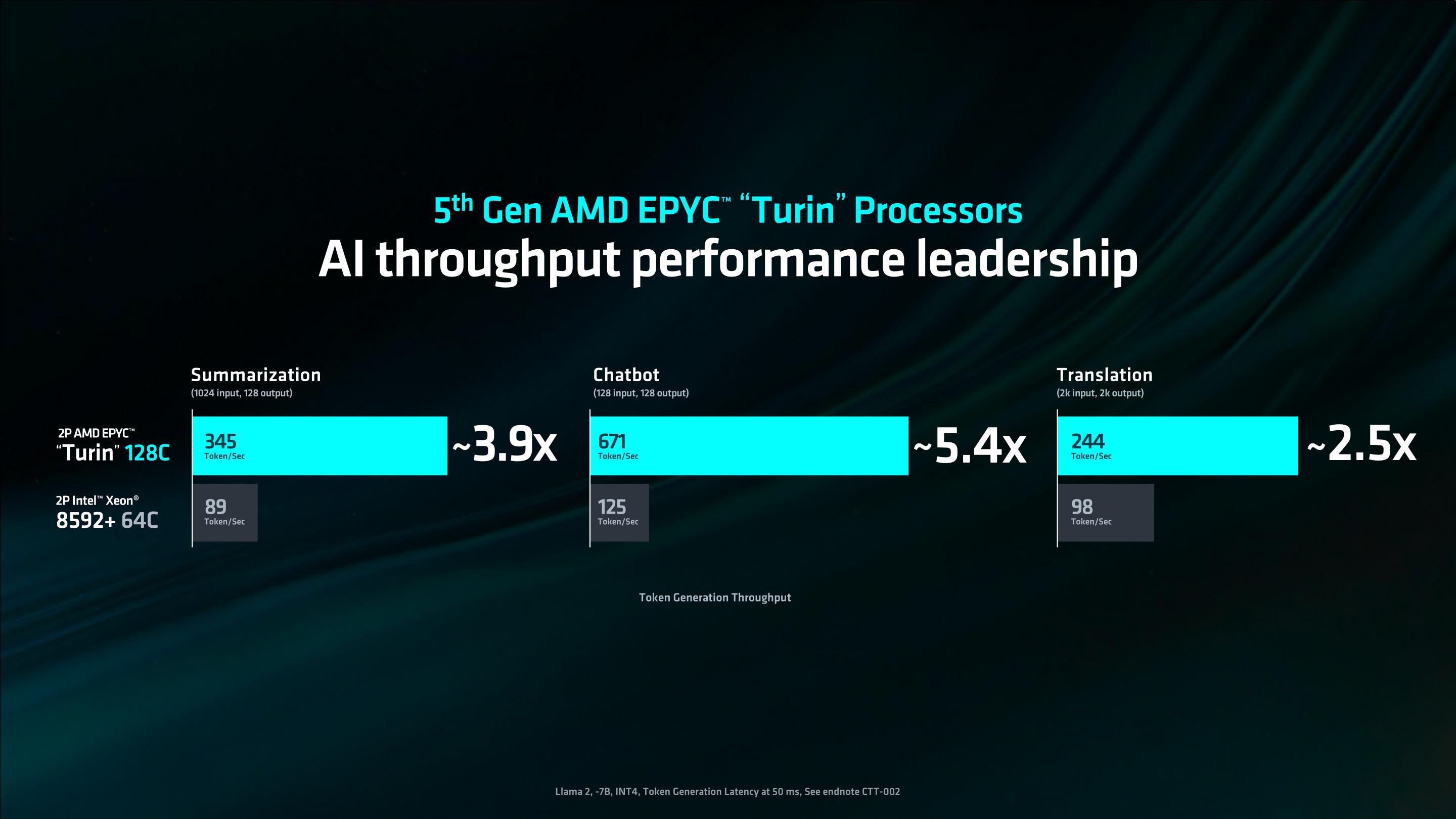
Hardware configurations aside, AMD also showcased a couple of benchmarks, pitting the new EPYC chips against Intel’s Xeons. As you’d expect in a keynote teaser, AMD was winning handily. Though it is interesting to note that the chips benchmarked were all 128 core Turins, rather than on the 192 core model being shown off today.

AMD will be shipping EPYC Turin in the second half of this year. More details on the chips and configurations will follow once AMD gets closer to the EPYC launch.

The Qualcomm Computex 2024 Keynote Live Blog (10:30pm PT/05:30 UTC)

3 juin 2024 à 05:10

For our second keynote of the day for Computex, we have the 4th Musketeer of the great PC powers, Qualcomm. Slated to be the most PC-focused of the four keynotes, company CEO Cristiano Amon will be presenting a keynote entitled “The PC Reborn.” And while Amon is no stranger to giving keynotes, this is slated to be his most PC-centric keynote yet, giving Computex attendees a clearer idea of how focused Qualcomm will be on the PC market with their new Windows-on-Arm SoCs.

The big focus for today's keynote is expected to be the Snapdragon X Elite and X Plus SoCs, which Qualcomm announced over half a year ago, and has been touting ever since. Now, the first consumer devices based on these chips are just a couple of weeks away from shipping, so Qualcomm is in their final promotional push for their new Windows-on-Arm platform. As a result, Qualcomm should have a lot more hardware to show off, with final silicon and shipping SKUs already defined.

While Snapdragon X is not Qualcomm’s first effort to ship an Arm-based SoC for Windows devices – there are 3 generations of 8cx Gen 3 platforms that everyone is happy never to mention again – the Snapdragon X is Qualcomm’s most serious effort yet. At its core is the new, high-performance/high-efficiency Oryon CPU core, which combined with the rest of Qualcomm’s tried-and-true mobile hardware experience, the company is hoping to mold into a revolutionary Arm-based SoC for Windows laptops. The company is also counting on a decade of software development on Microsoft’s part to make the Windows-on-Arm ecosystem whole, not to mention as frictionless as possible.

Besides energy efficiency, Qualcomm’s other big push is on the burgeoning field of NPUs. The Snapdragon X NPU is rated to deliver 45 TOPS of INT8 performance, which makes it the first PC NPU to meet Microsoft’s hardware requirement for Windows 11 Copilot+ AI functionality. So Qualcomm is looking to leverage this time-limited opportunity to be the first to offer new functionality in the Windows space – a privilege normally reserved for Intel or AMD.

Come join us at 10:30pm PT / 01:30am ET / 05:30 UTC to get all the details.

AMD Slims Down Compute With Radeon Pro W7900 Dual Slot For AI Inference

3 juin 2024 à 03:05

While the bulk of AMD’s Computex presentation was on CPUs and their Instinct lineup of dedicated AI accelerators, the company also has a small product refresh for the professional graphics and workstation AI crowd. AMD is releasing a dual-slot version of their high-end Radeon Pro W7900 card – aptly named the W7900 Dual Slot – with the intent being to improve compute density in workstations by making it possible to install 4 of the cards inside a single chassis.

The release of a dual-slot version of the card comes after the original Radeon Pro W7900 was the first time AMD went with a larger, triple-slot form factor for their flagship workstation card. With the W7000 generation bringing an all-around increase in power consumption, pushing the W7900 to 295 Watts, AMD originally opted to release a larger card for improved acoustics. However this came at the cost of compute density, as most systems could only fit 2 of the thicker cards. As a result, AMD is opting to release a dual-slot version of the hardware as well, to offer a more competitive product for high-density workstation systems – particularly those doing local AI inference.

AMD Radeon Pro Specification Comparison
  AMD Radeon Pro W7900DS AMD Radeon Pro W7900 AMD Radeon Pro W7800 AMD Radeon Pro W6800
ALUs 12288
(96 CUs)
8960
(70 CUs)
3840
(60 CUs)
ROPs 192 128 96
Boost Clock 2.495GHz 2.495GHz 2.32HHz
Peak Throughput (FP32) 61.3 TFLOPS 45.2 TFLOPS 17.8 TFLOPS
Memory Clock 18 Gbps GDDR6 18 Gbps GDDR6 16 Gbps GDDR6
Memory Bus Width 384-bit 256-bit 256-bit
Memiry Bandwidth 864GB/sec 576GB/sec 512GB/sec
VRAM 48GB 32GB 32GB
ECC Yes
(DRAM)
Yes
(DRAM)
Yes
(DRAM)
Infinity Cache 96MB 64MB 128MB
Total Board Power 295W 260W 250W
Manufacturing Process GCD: TSMC 5nm
MCD: TSMC 6nm
GCD: TSMC 5nm
MCD: TSMC 6nm
TSMC 7nm
Architecture RDNA3 RDNA3 RDNA2
GPU Navi 31 Navi 31 Navi 21
Form Factor Dual Slot Blower Triple Slot Blower Dual Slot Blower Dual Slot Blower
Launch Date 06/2024 Q2'2023 Q2'2023 06/2021
Launch Price (MSRP) $3499 $3999 $2499 $2249

Other than the narrower cooler, the Radeon Pro W7900DS is for all intents and purposes identical to the original W7900, with the same Navi 31 GPU being driven to the same clockspeeds, and the overall board being run to the same 295 Total Board Power (TBP) limit. This is paired with the same 18Gbps GDDR6 as before, giving the card 48GB of VRAM.

Officially, AMD doesn’t have a noise specification for these cards. But you can expect that the W7900DS will be louder than its triple-slot senior. By all appearances, AMD is just using the cooler from the W7800, which was a dual-slot card from the start, so that cooler is being tasked with handling another 35W of heat dissipation.

As the W7800 was also AMD’s fastest dual-slot card up until now, it’s an apt point of comparison for compute density. With its full-fat Navi 31 GPU, the W7900DS will offer about 36% more compute/pixel throughput than its sibling/predecessor. So it’s a not-insubstantial improvement for the very specific niche AMD has in mind for the card.

And like so many other things being announced at Computex this year, that niche is AI. While AMD offers PCIe versions of their Instinct MI210 accelerators, those cards are geared at servers, with fully-passive coolers to match. So workstation-level compute is largely picked up by AMD’s Radeon Pro workstation cards, which are intended to go into a traditional PC chassis and use active cooling (blowers). In this case, AMD is specifically going after local inference workloads, as that’s what the Radeon hardware and its significant VRAM pool are best suited for.

The Radeon Pro W7900 Dual Slot will drop on June 19th. Notably, AMD is introducing the card at a slightly lower price tag than they launched the original W7900 at last year, with the W7900DS hitting retail shelves at $3499, down from the W7900’s original $3999 price tag.

ROCm 6.1 For Radeons Coming as Well

Alongside the release of the W7900DS, AMD is also promoting the upcoming Radeon release of ROCm 6.1, their software stack for GPU computing. While baseline ROCm 6.1 was introduced back in April, the Windows version of AMD’s software stack is still a trailing (and feature limited) release. So that is slated to finally get bumped up to a ROCm 6.1 release on June 19th, the same day the W7900DS launches.

ROCm 6.1 for Radeons is slated to bring a couple of major changes/improvements to the stack, particularly when it comes to expanding the scope of available features. Notably, AMD will finally be shipping Windows Subsystem for Linux 2 (WSL2) support, albeit at a beta level, allowing Windows users to access the much richer feature set and software ecosystem of ROCm under Linux. This release will also incorporate improved support for multi-GPU configurations, perfect timing for the launch of the Radeon Pro W7900DS.

Finally, ROCm 6.1 sees TensorFlow integrated into the ROCm software stack as a first-class citizen. While this matter involves more complexities than can be summarized in a simple news story, native TensorFlow support under Windows was previously blocked by a lack of a Windows version of AMD’s MIOpen machine learning library. Combined with WSL2 support, developers will have two ways to access TensorFlow on Windows systems going forward.

AMD Launching New CPUs for AM4: Ryzen 5000XT Series Coming in July

3 juin 2024 à 03:04

During their opening keynote at Computex 2024, AMD announced their intention to launch a pair of new Ryzen 5000 processors for their legacy AM4 platform. The new chips, both getting the XT suffix, will be the Ryzen 9 5900XT, a 16 core Zen 3 part, while the Ryzen 7 5800XT will be an 8 core Zen 3.

The new chips are intended to underscore AMD's ongoing commitment to supporting their consumer platforms over several years. And while the specification changes are rather minor overall – the Zen 3 CPU architecture has long since been taken as far as it can reasonable go – it does give AMD a chance to refresh the platform by slinging hardware at new price points. AMD did something very similar for the Ryzen 3000 generation with the late-model Ryzen 3000 XT chips.

AMD Ryzen 5000XT Series Processors
(Zen 3)
AnandTech Cores /
Threads
Base
Freq
Turbo
Freq
L2
Cache
L3
Cache
TDP
Ryzen 9 5950X 16C / 32T 3.4 GHz 4.9 GHz 8 MB 64 MB 105 W
Ryzen 9 5900XT 16C / 32T 3.3 GHz 4.8 GHz 8 MB 64 MB 105 W
Ryzen 9 5900X 12C / 24T 3.7 GHz 4.8 GHz 6 MB 64 MB 105 W
Ryzen 7 5800XT 8C / 16T 3.8 GHz 4.8 GHz 4 MB 32 MB 105 W
Ryzen 7 5800X 8C / 16T 3.8 GHz 4.7 GHz 4 MB 32 MB 105 W

We've dedicated many column inches covering Zen 3 and the Ryzen 5000 series since they launched in late 2020, so there isn't anything new to add here. Zen 3 is no longer AMD's latest and greatest, but the platform as a whole is quite cheap to produce, making it a viable budget offering for new builds, or offering one last upgrade for old builds.

The Ryzen 9 5900XT is a 16 core part, and isn't to be confused with the Ryzen 9 5900X, which is a 12 core part. It ships with a peak turbo clockspeed of 4.8GHz, 100 MHz lower than the top-tier Ryzen 9 5950X. This makes it's XT designation somewhat of a misnomer compared to previous generations of XT chips, although it's clear that AMD has boxed themselves into a corner with their naming scheme, as they both need a way to designate that this is a new chip, and yet still place it below the 5950X.

Looking at the second chip, we have the Ryzen 7 5800XT. This is an 8 core part that does improve on its predecessor, offering a 4.8GHz max turbo clock that is 100MHz higher than the Ryzen 7 5800X's. Both chips otherwise share the same characteristics, including 6 MB of L2 cache and 32 MB of L3 cache, and all four of the chips – including the two new XT series and the corresponding X series chips – all come with a 105 Watt TDP.

In terms of motherboard compatibility, all of the AM4 motherboards that currently support the Ryzen 5000 series are also compatible with the Ryzen 5000XT series, although users are likely to need to perform a firmware update to ensure maximum compatibility; they are the same chips, but the microcodes are likely different.

AMD has provided some gaming performance figures comparing the Ryzen 9 5900XT to Intel's 13th Gen Core i7-13700K. It does offer very modest yet marginal gains in games by up to 4%; it's not mind-blowing, but the price could be the decisive factor here.

Regarding price, AMD hasn't disclosed anything official yet ahead of the expected launch of the Ryzen 5000XT series chips in July. It's hard to make a case for a pair of chips to be considered a fully-fledged series, but it does open up the doors for AMD to perhaps launch more 5000XT series chips in the future.

AMD Plans Massive Memory Instinct MI325X for Q4'24, Lays Out Accelerator Roadmap to 2026

3 juin 2024 à 03:02

In a packed presentation kicking off this year’s Computex trade show, AMD CEO Dr. Lisa Su spent plenty of time focusing on the subject of AI. And while the bulk of that focus was on AMD’s impending client products, the company is also currently enjoying the rapid growth of their Instinct lineup of accelerators, with the MI300 continuing to break sales projections and growth records quarter after quarter. It’s no surprise then that AMD is looking to move quickly then in the AI accelerator space, both to capitalize on the market opportunities amidst the current AI mania, as well as to stay competitive with the many chipmakers large and small who are also trying to stake a claim in the space.

To that end, as part of this evening’s announcements, AMD laid out their roadmap for their Instinct product lineup for both the short and long term, with new products and new architectures in development to carry AMD through 2026 and beyond.

On the product side of matters, AMD is announcing a new Instinct accelerator, the HBM3E-equipped MI325X. Based on the same computational silicon as the company’s MI300X accelerator, the MI325X swaps out HBM3 memory for faster and denser HBM3E, allowing AMD to produce accelerators with up to 288GB of memory, and local memory bandwidths hitting 6TB/second.

Meanwhile, AMD also showcased their first new CDNA architecture/Instinct product roadmap in two years, laying out their plans through 2026. Over the next two years AMD will be moving very quickly indeed, launching two new CDNA architectures and associated Instinct products in 2025 and 2026, respectively. The CDNA 4-powered MI350 series will be released in 2025, and that will be followed up by the even more ambitious MI400 series in 2026, which will be based on the CDNA "Next" architecture.

AMD Announces The Ryzen AI 300 Series For Mobile: Zen 5 With RDNA 3.5, and XDNA2 NPU With 50 TOPS

3 juin 2024 à 03:01

During AMD's opening keynote at Computex 2024, company CEO Dr. Lisa Su revealed AMD's latest AI PC-focused chip lineup for the mobile market, the Ryzen AI 300 series. Based on AMD's new Zen 5 CPU microarchitecture, the Ryzen AI 300 series – codenamed Strix Point – is intended to offer an across-the-board improvement in mobile SoC performance, with AMD proclaiming that the Ryzen AI 300 series will offer the fastest AI inference performance within the compact and portable PC market.

Under the hood, the new mobile SoC from AMD incorporates not only their new Zen 5 CPU architecture, but also their new RDNA 3.5-based integrated graphics, and the third generation XDNA2-based NPU, the latter of which is rated to deliver 50 TOPS of performance for AI-based workloads. As a result, the Ryzen AI 300 series represents a significant upgrade in AMD's mobile chip lineup, with all of the major aspects of the platform receiving a major upgrade versus their Zen 4-era Phoenix/Hawk Point SoCs. The one thing the new platform won't get, however, is a process node improvement; AMD is building Strix Point on a 4nm node, just like Phoenix/Hawk Point before it.

For this morning's announcement, AMD has unveiled the first two Ryzen AI 300 SKUs designed for notebooks. The first of these is the Ryzen AI 9 HX 370, which features 12 Zen 5 cores with a maximum boost frequency of up to 5.1 GHz, and comes equipped with 36 MB cache (12 MB L2 + 24 MB L3). The other chip to be announced is the Ryzen AI 9 365, which has two fewer Zen 5 cores (10 cores) and operates with a 5,0 GHz boost frequency and a 10 MB L2 + 24 MB L3 cache allocation.

AMD Unveils Ryzen 9000 CPUs For Desktop, Zen 5 Takes Center Stage at Computex 2024

3 juin 2024 à 03:00

During AMD's Computex 2024 kick-off keynote, AMD's CEO, Dr. Lisa Su, officially unveiled and announced the company's next generation of Ryzen processors. Today marks the first unveiling of AMD's highly anticipated Zen 5 microarchitecture via the Ryzen 9000 series, which is set to bring several advancements over Zen 4 and the Ryzen 7000 series for desktop PCs, which will launch sometime in July 2024.

AMD has unveiled four new chip SKUs using its Zen 5 microarchitecture. The AMD Ryzen 9 9950X processor will be the new consumer flagship part, featuring 16 CPU cores and a speedy 5.7 GHz maximum boost frequency. The other SKUs include, 6, 8, and 12 core parts, giving users a varied combination of core and thread counts. All four of these initial chips will be X-series chips, meaning they will have an unlocked multipliers and higher TDPs/clockspeeds.

In regards to performance, AMD is touting an average (geomean) IPC increase in desktop workloads for Zen 5 of 16%. And with the new desktop Ryzen chips' turbo clockspeeds remaining largely identical to their Ryzen 7000 predecessors, this should translate into similar performance expectations for the new chips.

The AMD Ryzen 9000 series will also launch on the AM5 socket, which debuted with AMD's Ryzen 7000 series and marks AMD's commitment to socket/platform longevity. Along with the Ryzen 9000 series will come a pair of new high-performance chipsets: the X870E (Extreme) and the regular X870 chipsets. The fundamental features that vendors will integrate into their specific motherboards remain tight-lipped. Still, we do know that USB 4.0 ports are standard on the X870E/X870 boards, along with PCIe 5.0 for both PCIe graphics and NVMe storage, with higher AMD EXPO memory profile support expected than previous generations.

The AMD Computex 2024 Keynote Live Blog (6:30pm PT/01:30 UTC)

3 juin 2024 à 01:00

Computex keynote season is kicking into high gear this morning with the show's leading keynote, which is being delivered by AMD. Company CEO Dr. Lisa Su will be presenting a keynote entitled “The future of high-performance computing in the AI era,” and with a run time of 90 minutes, we're expecting AMD to have a whole host of product announcements covering their full spectrum of product categories.

The big expectation here is fresh news around AMD’s Zen 5 CPU core architecture, and the chips built around it. AMD’s most recent Zen 5 roadmap has it slated to deliver all three flavors of Zen 5 by the end of this year, and we’re coming up on the two-year anniversary of the Zen 4 architecture launch.

Along with client chips, AMD has been pushing their server CPUs hard, and they’ve previously told investors that the next-gen EPYC Turin CPU is “looking great”. So we’ll likely hear about both client and server Zen 5 product plans during this keynote.

On the GPU/accelerator side of matters, AMD is mid-cycle (at best) with their Instinct MI300 series accelerators. With the company’s sales repeatedly beating their own expectations, AMD doesn’t seem to need much help moving this premium silicon right now. But with AI being the operative buzzword of this year’s Computex (and indeed, the computing industry as a whole), it would be weird for AMD to not have something to say about their rapidly growing AI accelerator product line.

Come join us at 6:30pm PT / 9:30pm ET / 01:30 UTC to get all the details.

Computex 2024 Keynote Preview: The Great PC Powers Convene

1 juin 2024 à 00:00

The annual Computex computer expo kicks off in Taepei this weekend. And this year’s show is shaping up to be the most packed in years.

Computex rivals CES for the most important PC trade show of the year, and in most years is attended by not only the numerous local Taiwanese firms (Asus, MSI, ASRock, and others), but the major chip developers have been increasing their own presence as well. These days, while CES itself tends to land more high-profile announcements, in recent years it’s been Computex that has delivered on more substantial announcements. This is largely because tech firms have aligned their product schedules to roll out near gear in the second half of the year, when retail sales are stronger due to the back-to-school and holiday shopping periods.

This year’s show, in turn, is looking to be an especially big year for the PC ecosystem. All the major PC chip firms – AMD, Intel, NVIDIA, and the 4th Musketeer, Qualcomm – are holding keynote addresses at this year’s show, where they’re expected to announce new slates of PC products to ship later this year. In a normal year there is typically only major announcements from one or two of the major chip firms, so having all four of them at the show delivering lengthy keynotes is setting things up for what should be an exceptional show.

TSMC's 3D Stacked SoIC Packaging Making Quick Progress, Eyeing Ultra-Dense 3μm Pitch In 2027

31 mai 2024 à 15:00

TSMC's 3D-stacked system-on-integrated chips (SoIC) advanced packaging technologies is set to evolve rapidly. In a presentation at the company's recent technology symposium, TSMC outlined a roadmap that will take the technology from a current bump pitch of 9μm all the way down to a 3μm pitch by 2027, stacking together combinations of A16 and N2 dies.

TSMC has a number of advanced packaging technologies, including 2.5D CoWoS and 2.5D/3D InFO. Perhaps the most intriguing (and complex) method is their 3D-stacked system-on-integrated chips (SoIC) technology, which is TSMC's implementation of hybrid wafer bonding. Hybrid bonding allows two advanced logic devices to be stacked directly on top of each other, allowing for ultra-dense (and ultra-short) connections between the two chips, and is primarily aimed at high performance parts. For now, SoIC-X (bumpless) is used for select applications, such as AMD's 3D V-cache technology for CPUs, as well as their Instinct MI300-series AI products. And while adoption is growing, the current generation of the technology is constrained by limitations on die sizes and interconnection pitches.

But those limitations are expected to give way quickly, if all goes according to plan for TSMC. SoIC-X technology is going to advance fast, and by 2027, it will be possible assemble a chip pairing a reticle-sized top die made on TSMC's leading-edge A16 (1.6nm-class) on a bottom die produced using TSMC's N2 (2nm-class). These dies, in turn, would be connected using 3μm bond pitche ssilicon vias (TSVs), three times the density of the size of today's 9μm pitch. Such small interconnections will allow for a much larger number of connections overall, greatly increasing the bandwidth density (and thus performance) of the assembled chip.

TSMC's SoIC-X Roadmap
Data by TSMC (Compiled by AnandTech)
  2022 2023 2024 2025 2026 2027
Top Die N7 N5 N4 N3 N2 A16
Bottom Die N7 ≥N6 ≥N5 ≥N4 ≥N3 ≥N2
Bond Pitch 9 μm 9 μm 6 μm 6 μm 4.5 μm 3 μm
Size* 0.1 reticle 0.4 reticle 0.8 reticle 1 reticle 1 reticle 1 reticle

*TSMC considers reticle size as roughly 830 mm2.

Improved hybrid bonding techniques are intended to allow TSMC's big HPC customers – AMD, Broadcom, Intel, NVIDIA, and the like – to build large, ultra-dense disaggregated processor designs for demanding applications, where distance between the dies is critical, as is the overall floor space used. Meanwhile, for applications where only performance matters, it will be possible to place multiple SoIC-X packages on a CoWoS interposer to get improved performance at a lower power consumption.

In addition to developing its bumpless SoIC-X packaging technology aimed at devices that require extreme performance, TSMC will also launch its bumped SoIC-P packaging process in the near future. SoIC-P is designed for cheaper lower performance applications that still want 3D-stacking, but don't need the additional performance and complexity that comes with bumpless copper-to-copper TSV connections. This packing technique will enable a broader range of companies to leverage SoIC, and while TSMC can't speak for their customers' plans, a cheaper version of the technology may make it accessible for more cost-conscious consumer applications.

Per TSMC's current plans, by 2025 the company will offer a face-to-back (F2B) bumped SoIC-P technology capable of pairing a 0.2-reticle sized N3 (3nm-class) top die with an N4 (4nm-class) bottom die, which will be connected using 25μm pitch microbumps (µbumps). In 2027, TSMC will introduce bumped face-to-face (F2F) SoIC-P technology, which will be able to place an N2 top die on an N3 bottom die with a pitch of 16μm.

TSMC's SoIC-P Roadmap
Data by TSMC (Compiled by AnandTech)
  2025 2027
Top Die N3 N2
Bottom Die ≥N4 ≥N3
Bond Pitch 25 μm 16 μm
Size* 0.2 reticle 0.4 reticle
Die Orientation face-to-back face-to-face
Qualification Time Q4 2024 for mobile SoC Q2 2026 for HPC

*TSMC considers reticle size as roughly 830 mm2

A lot of work has to be done to make SoIC more popular and accessible among chip developers, including continuing to iprove their die-to-die interfaces. But TSMC seems to be very optimistic about SoIC adoption by the industry, and expects around 30 SoIC designs to be released by 2026 – 2027.

GEEKOM A7 mini-PC Review : Premium Phoenix in a Compact 4x4 Package

31 mai 2024 à 12:00

The introduction of the Intel NUC in the early 2010s kickstarted the ultra-compact form-factor (UCFF) trend for desktop systems. Processors with TDPs ranging from 6 - 15W formed the backbone of this segment in the initial years. The emergence of configurable TDPs for notebook processors has prompted some vendors to introduce UCFF systems with regular 45W TDP processors (albeit, in cTDP-down mode).

GEEKOM, the private label brand of Shenzhen Jiteng Network Technology Co., has emerged as a popular UCFF system vendor in the last couple of years. After starting off with systems based on older processors, the company has moved on to introducing units carrying the latest and greatest from both AMD and Intel. The company has also been innovating on the form-factor side with compact boards smaller than the traditional 4"x4" ones in the NUC clones. The GEEKOM A7 is one such system based on AMD's Phoenix lineup.

The system is available in two configurations - one with the Ryzen 7 7840HS, and the other with the Ryzen 9 7940HS. The company sent over the flagship configuration to put through our evaluation routine for small form-factor computing systems. Read on to explore the performance profile and value proposition of the system, along with a discussion of the trade-offs involved in cramming a powerful notebook processor inside a system smaller than the traditional NUC.

TSMC: Performance and Yields of 2nm on Track, Mass Production To Start In 2025

30 mai 2024 à 19:00

In addition to revealing its roadmap and plans concerning its current leading-edge process technologies, TSMC also shared progress of its N2 node as part of its Symposiums 2024. The company's first 2nm-class fabrication node, and predominantly featuring gate-all-around transistors, according to TSMC N2 has almost achieved its target performance and yield goals, which places it on track to enter high-volume manufacturing in the second half of 2025.

TSMC states that 'N2 development is well on track and N2P is next.' In particular, gate-all-around nanosheet devices currently achieve over 90% of their expected performance, whereas yields of 256 Mb SRAM (32 MB) devices already exceeds 80%, depending on the batch. All of this for a node that is over a year away from mass production.

Meanwhile, average yield of a 256 Mb SRAM was around 70% as of March, 2024, up from around 35% in April, 2023. Device performance has also been improving with higher frequencies being achieved while keeping power consumption in check.

Chip designer interest towards TSMC's first 2nm-class gate-all-around nanosheet transistor-based technology is significant, too. The number of new tape-outs (NTOs) in the first year of N2 is over two-times higher than it was for N5. Though with that said, given TSMC's close working relationship with a handful of high-volume vendors – most notably Appe – NTOs can be a very misleading figure since the first year of a new node at TSMC is capacity constrained, and consequently the bulk of that capacity goes to TSMC's priority partners.

Meanwhile, there were considerably more N5 tapeouts in its second year (some where N5P, of course) and N2 promises to have 2.6X more NTOs in its second year. So the node indeed looks quite promising. In fact, based on TSMC's slides (which we're unfortunately not able to republish), N2 is more popular than N3 in terms of NTOs both in the first and the second years of existence.

When it comes to the second year of N2, in the second half of 2026 TSMC plans to roll out its N2P technology, which promises additional performance and power benefits. N2P is expected to improve frequency by 15% - 20%, reduce power consumption by 30% - 40%, and increase chip density by over 1.15 times compared to N3E, significant benefits to move to all-new GAA nanosheet transistors.

Finally, for those companies that need the best in performance, power, and density, TSMC is poised to offer their A16 process in 2026. That node will also bring in backside power delivery, which will add costs, but is expected to greatly improve performance efficiency and scaling.

Lexar ARMOR 700 Portable SSD Review: Power-Efficient 2 GBps in an IP66 Package

30 mai 2024 à 12:00

Lexar has a long history of serving the flash-based consumer storage market in the form of SSDs, memory cards, and USB flash drives. After having started out as a Micron brand, the company was acquired by Longsys which has diversified its product lineup with regular introduction of new products. Recently, the company announced a number of portable SSDs targeting different market segments. The Lexar ARMOR 700 Portable SSD makes its entry as the new flagship in the 20 Gbps PSSD segment.

Despite its flagship positioning and rugged nature, the ARMOR 700 is reasonably priced thanks to the use of a native USB flash controller - the Silicon Motion SM2320. Similar to the SL500, the product uses YMTC 3D TLC NAND (compared to the usual Micron or BiCS NAND that we have seen in SM2320-based PSSDs from other vendors). Read on for a detailed look at the ARMOR 700, including an analysis of its internals and evaluation of its performance consistency, power consumption, and thermal profile.

Arm Unveils 2024 CPU Core Designs, Cortex X925, A725 and A520: Arm v9.2 Redefined For 3nm

29 mai 2024 à 15:00

As the semiconductor industry continues to evolve, Arm stands at the forefront of innovation for its core and IP architecture, especially in the mobile space, by pushing the boundaries of technology to deliver cutting-edge solutions for end users. For 2024, Arm's year-on-year strategic advancements focus on enhancing last year's Armv9.2 architecture with a new twist. Arm has rebranded and re-strategized its efforts by introducing Arm Compute Subsystem (CSS), the direct successor to last year's Total Compute Solutions (TSC2023) platform.

Arm is also transitioning its latest IP and Cortex core designs, including the largest Cortex X925, the middle Cortex A725, and the refreshed and smaller Cortex A520 to the more advanced 3 nm process technology. Arm promises that the 3 nm process node will deliver unprecedented performance gains compared to last year's designs, power efficiency and scalability improvements, and new front and back-end refinements to its Cortex series of cores. Arms' new solutions look to power the next-generation mobile and AI applications as Arm, along with its complete AArch64 64-bit instruction execution and approach to solutions geared towards mobile and notebooks, look set to redefine end users' expectations within the Android and Windows on Arm products.

❌
❌