Vue lecture

Il y a de nouveaux articles disponibles, cliquez pour rafraîchir la page.

ASRock Unveils Motherboards For Ryzen 9000 At Computex 2024: X870E Taichi and X870E Taichi Lite

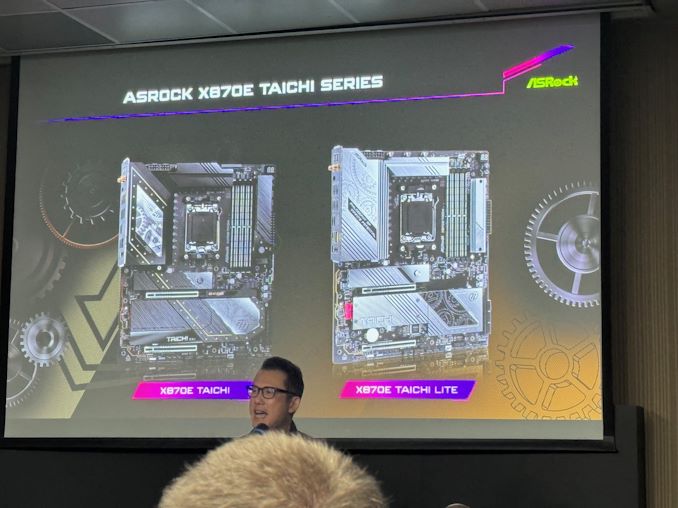
During Computex 2024, ASRock held an event to unveil some of its upcoming X870E motherboards, designed for AMD's Zen 5-based Ryzen 9000 series processors. ASRock's announcement includes a pair of Taichi-branded boards, the X870E Taichi and the lighter X870E Taichi lite, which uses AMD's X870E (Promontory 21) chipset for AM5.

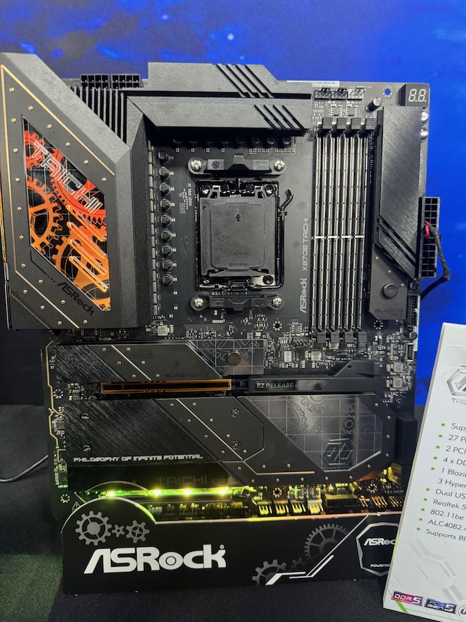
The current flagship model announced from ASRock's X870E line-up for Ryzen 9000 is the ASRock X870E Taichi. ASRock is advertising a large 27-phase power delivery through 110A SPS, suggesting this board is designed for overclockers and all-around power users. Two PCIe 5.0 x16 slots (operating in either x16/x0 or x8/x8) provide high-speed bandwidth for cutting-edge graphics cards and other devices. Meanwhile, ASRock has gone with 4 DIMM slots on this board, so system builders will be able to max out the board's memory capacity at the cost of bandwidth.

The storage offering is impressive; besides the obligatory PCIe Gen5 x4 M.2 slot (Blazing M.2), ASRock has outfit the board with another three PCIe Gen4 x4 (Hyper) M.2 slots. Also present are two USB4 Type-C ports for high-bandwidth external I/O, while networking support is a solid pairing of a discrete Wi-Fi 7 controller with a Realtek 5Gb Ethernet controller (and the first AM5 board we've come across with something faster than a 2.5GbE controller).

The audio setup includes a Realtek ALC4082 codec and ESS SABRE9218 DAC supporting high-fidelity sound. The BIOS flashback feature is also a nice touch, and we believe this should be a feature on all mid-range to high-end motherboards, which provides an easy way to update the firmware without installing a CPU. And, as no high-end board would be complete without it, ASRock has put RGB lighting on the X870E Taichi as well.

Ultimately, as ASRock's high-end X870E board, the X870E Taichi comes with pretty much every last cutting-edge technology that ASRock can fit on the board.

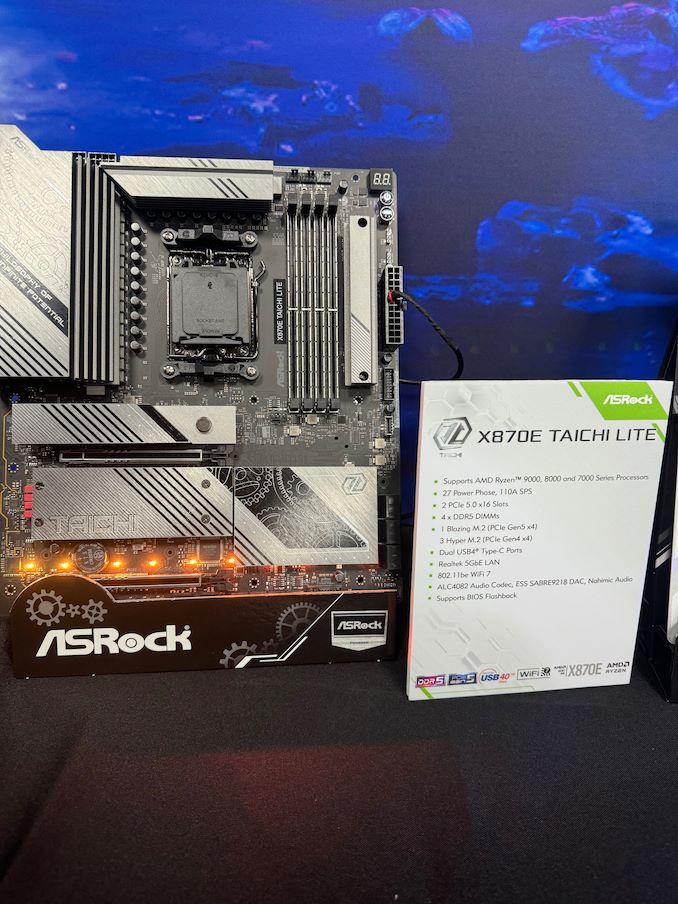
Comparatively, the ASRock X870E Taichi Lite is a more streamlined and functional version of the X870E Taichi. The Lite retaining all of the latter's key features, including the 27-phase power delivery with 110A smart power stages, dual PCIe 5.0 x16 slots operating at x16 or x8/x8, four DDR5 DIMM slots, and four M.2 slots (1x Gen5 + 3x Gen4). The only significant difference is aesthetics: the Taichi Lite features a simpler silver-themed design without the RGB lighting, while the standard Taichi has a more intricate gold-accented and fanciful aesthetics.

In terms of availability, ASRock is not disclosing a release date for the board at the show. And, checking around with other tech journalists, Andreas Schilling from HawrdwareLUXX has heard that X870E and X870 motherboards aren't expected to be available in time for the Ryzen 9000 series launch. We will investigate this and contact the motherboard vendors to confirm the situation. Though as X870E/X870 boards barely differ from the current crop of X670E/B650E boards to begin with, the Ryzen 9000 series won't be fazed by a lack of slightly newer motherboards.

MSI Teases Z790 Project Zero Plus Motherboard With CAMM2 Memory Support

MSI on Thursday published the first image of a new desktop motherboard that supports the innovative DDR5 compression attached memory module (CAMM2). DDR5 CAMM2 modules are designed to improve upon the SO-DIMM form factor used for laptops, alleviating some of the high-speed signaling and capacity limitations of SO-DIMMs while also shaving down on the volume of space required. And while we're eagerly awaiting to see CAMM2 show up in more laptops, its introduction in a PC motherboard comes as a bit of a surprise, since PCs aren't nearly as space-constrained.

MSI's Z790 Project Zero Plus motherboard, which supports Intel's latest 14th Generation Core processors, is to a large degree a proof-of-concept product that is showcasing several new technologies and atypical configuration options. Key among these, of course, is the CAMM2 connector. The single connector supports a 128-bit DDR5 memory bus, allowing for a system to be fully populated with RAM with just a single, horizontally-mounted CAMM2 module. And in terms of design, the Zero Plus also features backside power connectors for improved cable management.

CAMM2 is designed to replace traditional modules in an SO-DIMM form-factor and is meant to occupy up to 64% less space than two DDR5 SO-DIMMs. In addition, CAMM2 greatly optimizes signal and power traces inside the motherboard, primarily by ensuring all memory trace lengths are identical, reducing some of the signaling penalties that normally come from supporting multiple SO-DIMM slots in a system. With DDR5 being particularly sensitive here – to the point where 2 DIMM Per Channel (2DPC) configurations take a max frequency hit even on desktop systems – CAMM2 modules are expected to simplify and, to a degree, improve laptop designs to better match DDR5's limitations.

Though whether CAMM2 sees widespread adoption remains to be seen. Unlike it's LPDDR5X counterpart, LPCAMM2, DDR5 CAMM2 hasn't attracted the same interest from laptop vendors quite yet, in large part because it doesn't introduce any new functionality (e.g. socketed LPDDR5X).

Meanwhile CAMM2 in ATX desktops is all but unexplored right now, which is why we're seeing experimental products like MSI's motherboard. The space savings alone aren't as important in desktops due to their size – though CAMM2 does cut down on Z-height, keeping memory away from CPU coolers. But PC makers will be looking at other factors such as inventory, as equipping desktop boards with CAMM2 connectors would allow them to use the same memory modules in both laptops and desktops. And longer term there is the question of whether CAMM2 can deliver tangible signaling benefits over traditional DIMMs.

MSI plans to showcase its Z790 Project Zero Plus platform at Computex, alongside memory partner Kingston. The latter will be at the show to demonstrate its Fury Impact CAMM2 memory module, which is one of the first DDR5 CAMM2 modules to be announced.

Samsung Starts Mass Production of 9th Generation V-NAND: 1Tb 3D TLC NAND

Samsung Electronics has started mass production of its 9th generation of V-NAND memory. The first dies based on their latest NAND tech come in a 1 Tb capacity using a triple-level cell (TLC) architecture, with data transfer rates as high as 3.2 GT/s. The new 3D TLC NAND memory will initially be used to build high-capacity and high-performance SSDs, which will help to solidify Samsung's position in the storage market.

Diving right in, Samsung is conspicuously avoiding to list the number of layers in their latest generation NAND, which is the principle driving factor in increasing capacity generation-on-generation. The company's current 8th gen V-NAND is 236 layers – similar to its major competitors – and word on the street is that 9th gen V-NAND ups that to 290 layers, though this remains to be confirmed.

Regardless, Samsung says that its 9th generation V-NAND memory boasts an approximate 50% improvement in bit density over its 8th generation predecessor. Driving this gains, the company cites the miniaturization of the cell size, as well as the integration of enhanced memory cell technologies that reduce interference and extend the lifespan of the cells. With their latest NAND technology, Samsung has also been able to eliminate dummy channel holes, thus reducing the planar area of the memory cells.

Interestingly, today's announcement also marks the first time that Samsung has publicly confirmed their use of string stacking in their NAND, referring to it as their "double-stack structure." The company is widely believed to have been using sting stacking back in their 8th generation NAND as well, however this was never confirmed by the company. Regardless, the use of string stacking is only going to increase from here, as vendors look to keep adding layers to their NAND dies, while manufacturing variability and channel hole tolerances make it difficult to produce more than 150-200 layers in a single stack.

Samsung TLC V- NAND Flash Memory
  9th Gen V-NAND 8th Gen V-NAND
Layers 290? 236
Decks 2 (x145) 2 (x118)
Die Capacity 1 Tbit 1 Tbit
Die Size (mm2) ?mm2 ?mm2
Density (Gbit/mm2) ? ?
I/O Speed 3.2 GT/s
(Toggle 5.1)
2.4 GT/s
(Toggle 5.0)
Planes 6? 4
CuA / PuC Yes Yes

Speaking of channel holes, another key technological enhancement in the 9th gen V-NAND is Samsung's advanced 'channel hole etching' technology. This process improves manufacturing productivity by enabling the simultaneous creation of electron pathways within a double-stack structure. This method is crucial as it enables efficient drilling through more layers, which is increasingly important as cell layers are added.

The latest V-NAND also features the introduction of a faster NAND flash interface, Toggle DDR 5.1, which boosts peak data transfer rates by 33% to 3.2 GT/s, or almost 400MB/sec for a single die. Additionally, 9th gen V-NAND's power consumption has been reduced by 10%, according to Samsung. Though Samsung doesn't state under what conditions – presumably, this is at iso-frequency rather than max frequency.

Samsung's launch of 1Tb TLC V-NAND is set to be followed by the release of a quad-level cell (QLC) model later this year.

"We are excited to deliver the industry’s first 9th-gen V-NAND which will bring future applications leaps forward," said SungHoi Hur, Head of Flash Product & Technology of the Memory Business at Samsung Electronics. "In order to address the evolving needs for NAND flash solutions, Samsung has pushed the boundaries in cell architecture and operational scheme for our next-generation product. Through our latest V-NAND, Samsung will continue to set the trend for the high-performance, high-density solid-state drive (SSD) market that meets the needs for the coming AI generation."

❌