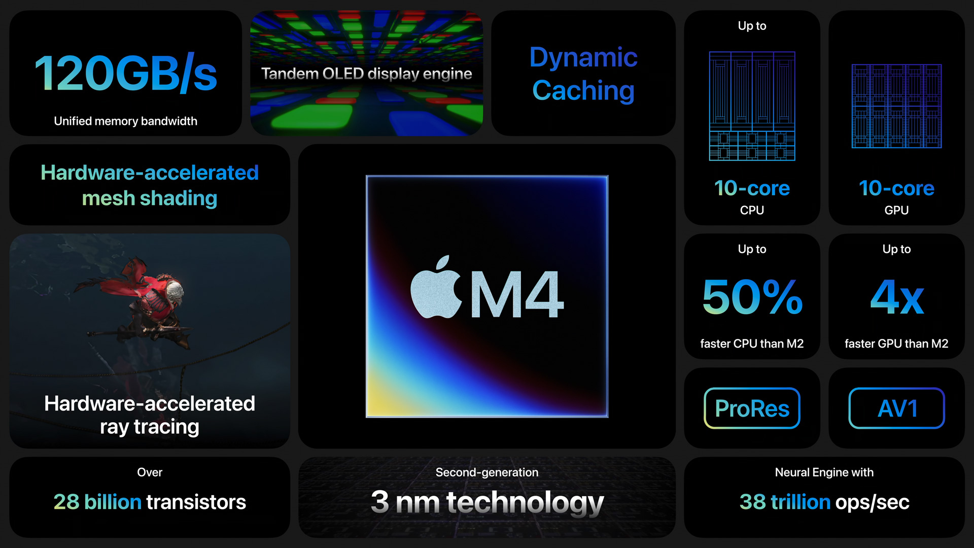
Setting things up for what is certainly to be an exciting next few months in the world of CPUs and SoCs, Apple this morning has announced their next-generation M-series chip, the M4. Introduced just over six months after the M3 and the associated 2023 Apple MacBook family, the M4 is going to start its life on a very different track, launching alongside Apple’s newest iPad Pro tablets. With their newest chip, Apple is promising class-leading performance and power efficiency once again, with a particular focus on machine learning/AI performance.
The launch of the M4 comes as Apple’s compute product lines have become a bit bifurcated. On the Mac side of matters, all of the current-generation MacBooks are based on the M3 family of chips. On the other hand, the M3 never came to the iPad family – and seemingly never will. Instead, the most recent iPad Pro, launched in 2022, was an M2-based device, and the newly-launched iPad Air for the mid-range market is also using the M2. As a result, the M3 and M4 exist in their own little worlds, at least for the moment.
Given the rapid turn-around between the M3 and M4, we’ve not come out of Apple’s latest announcement expecting a ton of changes from one generation to the next. And indeed, details on the new M4 chip are somewhat limited out of the gate, especially as Apple publishes fewer details on the hardware in its iPads in general. Coupled with that is a focus on comparing like-for-like hardware – in this case, M4 iPads to M2 iPads – so information is thinner than I’d like to have. None the less, here’s the AnandTech rundown on what’s new with Apple’s latest M-series SoC.
| Apple M-Series (Vanilla) SoCs |
| SoC |
M4 |
M3 |
M2 |
| CPU Performance |
4-core |
4-core |
4-core (Avalanche)
16MB Shared L2 |
| CPU Efficiency |
6-core |
4-core |
4-core (Blizzard)
4MB Shared L2 |
| GPU |
10-Core
Same Architecture as M3 |
10-Core
New Architecture - Mesh Shaders & Ray Tracing |
10-Core
3.6 TFLOPS |
| Display Controller |
2 Displays? |
2 Displays |
2 Displays |
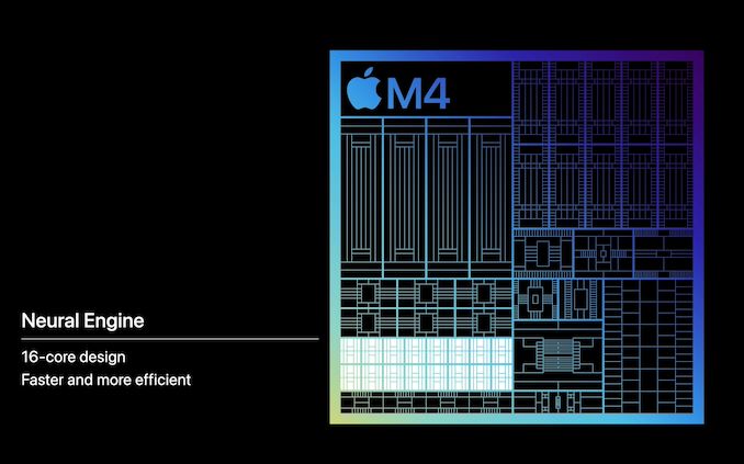
| Neural Engine |
16-Core
38 TOPS (INT8?) |
16-Core
18 TOPS |
16-Core
15.8 TOPS |
Memory
Controller |
LPDDR5X-7700
8x 16-bit CH
120GB/sec Total Bandwidth (Unified) |
LPDDR5-6400
8x 16-bit CH
100GB/sec Total Bandwidth (Unified) |
LPDDR5-6400
8x 16-bit CH
100GB/sec Total Bandwidth (Unified) |
| Max Memory Capacity |
24GB? |
24GB |
24GB |
Encode/
Decode |
8K
H.264, H.265, ProRes, ProRes RAW, AV1 (Decode) |
8K
H.264, H.265, ProRes, ProRes RAW, AV1 (Decode) |
8K
H.264, H.265, ProRes, ProRes RAW |
| USB |
USB4/Thunderbolt 3
? Ports |
USB4/Thunderbolt 3
2x Ports |
USB4/Thunderbolt 3
2x Ports |
| Transistors |
28 Billion |
25 Billion |
20 Billion |
| Mfc. Process |
TSMC N3E |
TSMC N3B |
TSMC N5P |
At a high level, the M4 features some kind of new CPU complex (more on that in a second), along with a GPU that seems to be largely lifted from the M3 – which itself was a new GPU architecture. Of particular focus by Apple is the neural engine (NPU), which is still a 16-core design, but now offers 38 TOPS of performance. And memory bandwidth has been increased by 20% as well, helping to keep the more powerful chip fed.
One of the few things we can infer with a high degree of certainty is the manufacturing process being used here. Apple’s description of a “second generation 3nm process” lines up perfectly in timing with TSMC’s second-generation 3nm process, N3E. The enhanced version of their 3nm process node is a bit of a sidegrade to the N3B process used by the M3 series of chips; N3E is not quite as dense as N3B, but according to TSMC it offers slightly better performance and power characteristics. The difference is close enough that architecture plays a much bigger role, but in the race for energy efficiency, Apple will take any edge they can get.
Apple’s position as TSMC’s launch-partner for new process nodes has been well-established over the years, and Apple appears to be the first company out the door launching chips on the N3E process. They will not be the last, however, as virtually all of TSMC’s high-performance customers are expected to adopt N3E over the next year. So Apple’s immediate chip manufacturing advantage, as usual, will only be temporary.
Apple’s early-leader status likely also plays into why we’re seeing the M4 now for iPads – a relatively low volume device at Apple – and not the MacBook lineup. At some point, TSMC’s N3E production capacity will catch up, and then-some. I won’t hazard a guess as to what Apple has planned for that lineup at that point, as I can’t really see Apple discontinuing M3 chips so quickly, but it also leaves them in an awkward spot having to sell M3 Macs when the M4 exists.
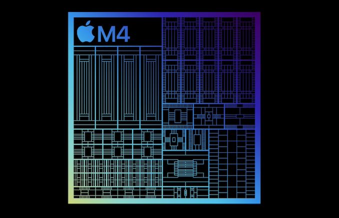
No die sizes have been quoted for the new chip (or die shots posted), but at 28 billion transistors in total, it’s only a marginally larger transistor count than the M3, indicating that Apple hasn’t thrown an excessive amount of new hardware into the chip. (ed: does anyone remember when 3B transistors was a big deal?)
M4 CPU Architecture: Improved ML Acceleration
Starting on the CPU side of things, we’re facing something of an enigma with Apple’s M4 CPU core design. The combination of Apple’s tight-lipped nature and lack of performance comparisons to the M3 means that we haven’t been provided much information on how the CPU designs compare. So if M4 represents a watershed moment for Apple’s CPU designs – a new Monsoon/A11 – or a minor update akin to the Everest CPU cores in A17, remains to be seen. Certainly we hope for the latter, but absent further details, we’ll work with what we do know.
Apple’s brief keynote presentation on the SoC noted that both the performance and efficiency cores implement improved branch predication, and in the case of performance cores, a wider decode and execution engine. However these are the same broad claims that Apple made for the M3, so this is not on its own indicative of a new CPU architecture.
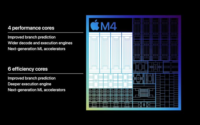
What is unique to Apple’s M4 CPU claims however are “next-generation ML accelerators” for both CPU core types. This goes hand-in-hand with Apple’s broader focus on ML/AI performance in the M4, though the company isn’t detailing on just what these accelerators entail. With the NPU to do all of the heavy lifting, the purpose of AI enhancements on the CPU cores is less about total throughput/performance and more about processing light inference workloads mixed inside more general-purpose workloads without having to spend the time and resources firing up the dedicated NPU.
A grounded guess here would be that Apple has updated their poorly-documented AMX matrix units, which have been a part of the M series of SoCs since the beginning. However recent AMX versions already support common ML number formats like FP16, BF16, and INT8, so if Apple has made changes here, it’s not something simple and straightforward such as adding (more) common formats. At the same time if it is AMX, it’s a bit surprising to see Apple mention it at all, since they are otherwise so secretive about the units.
The other reasonable alternative would be that Apple has made some changes to their SIMD units within their CPUs to add common ML number formats, as these units are more directly accessible by developers. But at the same time, Apple has been pushing developers to use higher-level frameworks to begin with (which is how AMX is accessed), so this could really go either way.
In any case, whatever the CPU cores are that underpin M4, there is one thing that is certain: there are more of them. The full M4 configuration is 4 performance cores paired with 6 efficiency cores, 2 more efficiency cores than found on the M3. Cut-down iPad models get a 3P+6E configuration, while the higher-tier configurations get the full 4P+6E experience – so the performance impact there will likely be tangible.
Everything else held equal, the addition of two more efficiency cores shouldn’t massively improve on CPU performance over the M3’s 4P+4E configuration. But then Apple’s efficiency cores should not be underestimated, as even Apple’s efficiency cores are relatively powerful thanks to their use of out-of-order execution. Especially when fixed workloads can be held on the efficiency cores and not promoted to the performance cores, there’s a lot of room for energy efficiency gains.
Otherwise, Apple hasn’t published any detail performance graphs for the new SoC/CPU cores, so there’s little in the way of hard numbers to talk about. But the company is claiming that the M4 delivers 50% faster CPU performance than the M2. This presumably is for a multi-threaded workload that can leverage the M4’s CPU core count advantage. Alternatively, in their keynote Apple is also claiming that they can deliver M2 performance at half the power, which as a combination of process node improvements, architectural improvements, and CPU core count increases, seems like a reasonable claim.
As always, however, we’ll have to see how independent benechmarks pan out.
M4 GPU Architecture: Ray Tracing & Dynamic Caching Return
Compared to the CPU situation on the M4, the GPU situation is much more straightforward. Having just recently introduced a new GPU architecture in the M3 – a core type that Apple doesn’t iterate on as often as the CPU – Apple has all but confirmed that the GPU in the M4 is the same architecture that was found in the M3.
With 10 GPU cores, at a high level the configuration is otherwise identical to what was found on the M3. Whether that means the various blocks and caches are truly identical to the M3 remains to be seen, but Apple isn’t making any claims about the M4’s GPU performance that could be in any way interpreted as it being superior to the M3’s GPU. Indeed, the smaller form factor of the iPad and more limited cooling capabilities means that the GPU is going to be thermally constrained under any sustained workload to begin with, especially compared to what the M3 can do in an actively-cooled device like the 14-Inch MacBook Pro.
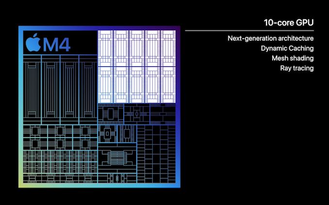
At any rate, this means the M4 comes with all of the major new architectural features introduced with the M3’s GPU: ray tracing, mesh shading, and dynamic caching. Ray tracing needs little introduction at this point, while mesh shading is a significant, next-generation means of geometry processing. Meanwhile, dynamic caching is Apple’s term for their refined memory allocation technique on M-series chips, which avoids over-allocating memory to the GPU from Apple’s otherwise unified memory pool.
GPU rendering aside, the M4 also gets the M3’s updated media engine block, which coming from the M2 is a relatively big deal for iPad uses. Most notably, the M3/M4’s media engine block added support for AV1 video decoding, the next-generation open video codec. And while Apple is more than happy to pay royalties on HEVC/H.265 to ensure it’s available within their ecosystem, the royalty-free AV1 codec is expected to take on a lot of significance and use in the coming years, leaving the iPad Pro in a better position to use the newest codec (or, at least, not have to inefficiently decode AV1 in software).
What is new to the M4 on the display side of matters, however, is a new display engine. The block responsible for compositing images and driving the attached displays on a device, Apple never gives this block a particularly large amount of attention, but when they do make updates to it, it normally comes with some immediate feature improvements.
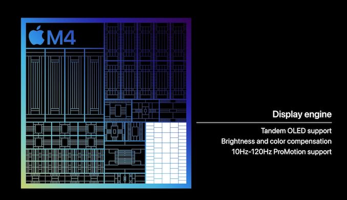
The key change here seems to be enabling Apple’s new sandwiched “tandem” OLED panel configuration, which is premiering in the iPad Pro. The iPad’s Ultra Retina XDR display places two OLED panels directly on top of each other in order allow for a display that can cumulatively hit Apple’s brightness target of 1600 nits – something that a single one of their OLED panels is apparently incapable of doing. This in turn requires a display controller that knows how to manipulate the panels, not just driving a mirrored set of displays, but accounting for the performance losses that would stem from having one panel below another.
And while not immediately relevant to the iPad Pro, it will be interesting to see if Apple used this opportunity to increase the total number of displays the M4 can drive, as vanilla M-series SoCs have normally been limited to 2 displays, much to the consternation of MacBook users. The fact that the M4 can drive the tandem OLED panels and an external 6K display on top of that is promising, but we’ll see how this translates to the Mac ecosystem if and when the M4 lands in a Mac.
M4 NPU Architecture: Something New, Something Faster
Arguably Apple’s biggest focus with the M4 SoC is the company’s NPU, otherwise known as their neural engine. The company has been shipping a 16-core design since the M1 (and smaller designs on the A-series chips for years before that), each generation delivering a modest increase in performance. But with the M4 generation, Apple says they are delivering a much bigger jump in performance.
Still a 16-core design, the M4 NPU is rated for 38 TOPS, just over twice that of the 18 TOPS neural engine in the M3. And coincidentally, only a few TOPS more than the neural engine in the A17. So as a baseline claim, Apple is pitching the M4 NPU as being significantly more powerful than what’s come in the M3, never mind the M2 that powers previous iPads – or going even farther back, 60x faster than the A11’s NPU.
Unfortunately, the devil is (once again) in the details here as Apple isn’t listing the all-important precision information – whether this figure is based on INT16, INT8, or even INT4 precision. As the precision de jure for ML inference right now, INT8 is the most likely option, especially as this is what Apple quoted for the A17 last year. But freely mixing precisions, or even just not disclosing them, is headache-inducing to say the least. And it makes like-for-like specification comparisons difficult.
In any case, even if most of this performance improvement comes from INT8 support versus INT16/FP16 support, the M4 NPU is slated to deliver significant performance improvements to AI performance, similar to what’s already happened with the A17. And as Apple was one of the first chip vendors to ship a consumer SoC with what we now recognize as an NPU, the company isn’t afraid to beat its chest a bit on the matter, especially comparing it to what is going on in the PC realm. Especially as Apple’s offering is a complete hardware/software ecosystem, the company has the advantage of being able mold their software around using their own NPU, rather than waiting for the killer app to be invented for it.
M4 Memory: Adopting Faster LPDDR5X
Last, but certainly not least, the M4 SoC is also getting a notable improvement in its memory capabilities. Given the memory bandwidth figures Apple is quoting for the M4 – 120GB/second – all signs point to them finally adopting LPDDR5X for their new SoC.
The mid-generation update to the LPDDR5 standard, LPDDR5X allows for higher memory clockspeeds than LPDDR5, which topped out at 6400 MT/second. While LPDDR5X is available at speeds up to 8533 MT/second right now (and faster speeds to come), based on Apple’s 120GB/second figure for the M4, this puts the memory clockspeed at roughly LPDDR5X-7700.
Since the M4 is going into an iPad first, for the moment we don’t have proper idea of its maximum memory capacity. The M3 could house up to 24GB of memory, and while it’s highly unlikely Apple has regressed here, there’s also no sign whether they’ve been able to increase it to 32GB, either. In the meantime, the iPads Pro will all either come with 8GB or 16GB of RAM, depending on the specific model.
2024 M4 iPad Pros: Coming Next Week
Wrapping things up, in traditional Apple fashion, prospective tablet buyers will get the chance to see the M4 in action sooner than later. The company has already opened up pre-orders for the new iPad Pros, with the first deliveries slated to take place next week, on May 15th.

Apple is offering two sizes of the 2024 iPad Pro: 11 inches and 13 inches. Screen size aside, both sizes are getting access to the same M4 and memory configurations. 256GB/512GB models get a 3P+6E core CPU configuration and 8GB of RAM, meanwhile the 1TB and 2TB models get a fully-enabled M4 SoC with a 4P+6E CPU configuration and 16GB of RAM. The GPU configuration on both models is identical, with 10 GPU cores.
Pricing starts at $999 for the 256GB 11-inch model and $1299 for the 256GB 13-inch model. Meanwhile a max-configuration 13-inch model with 2TB of storage, Apple’s nano-texture matte display, and cellular capabilities will set buyers back a cool $2599.